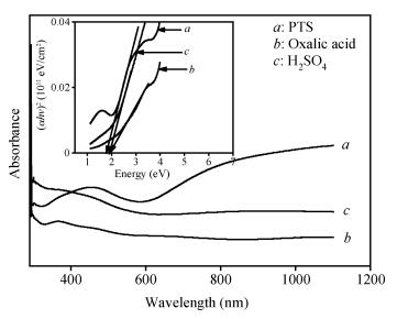
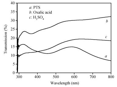
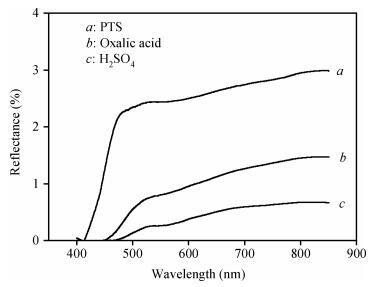
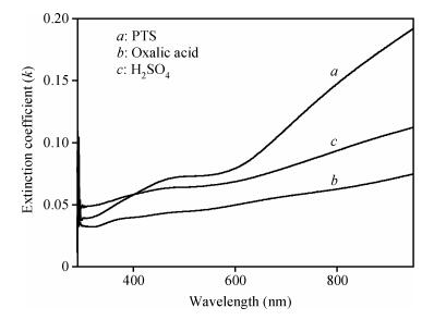
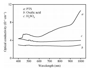
Polypyrrole thin films are prepared by the potentiostatic mode of electrodeposition at +0.7 V versus a saturated calomel electrode (SCE). The polypyrrole films are prepared in the presence of different electrolytes such as:p-toluene sulphonic acid (PTS), oxalic acid and H2SO4. The prepared films are characterized by UV-vis absorption spectroscopy and normal reflectance measurements. The electrochemically synthesized films are semiconductor in nature. The band gap energy of polypyrrole thin films is found to be 1.95, 1.92 and 1.79 eV for H2SO4, oxalic acid and p-toluene sulphonic acid, respectively. The normal reflectance spectroscopy of polypyrrole films shows that the maximum reflectance is in the presence of p-toluene sulphonic acid; this is may be due to a more distinct microstructure than the others. The optical constants such as the extinction coefficient, refractive index, optical conductivity, etc. are calculated and studied with various electrolytes.


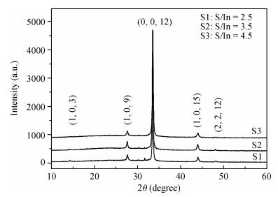
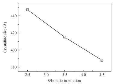
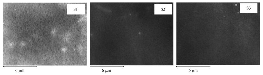
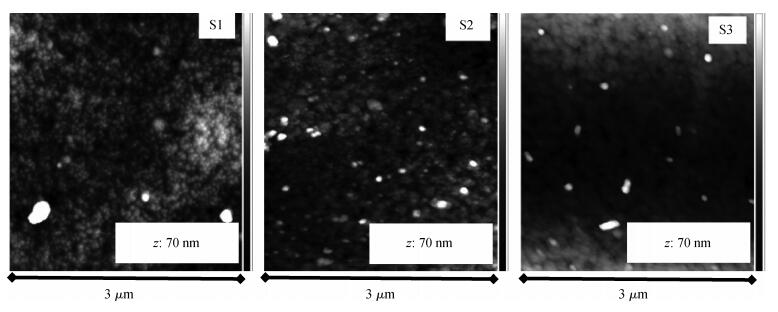
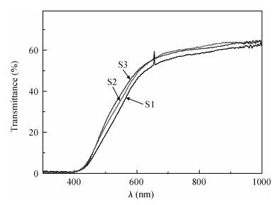
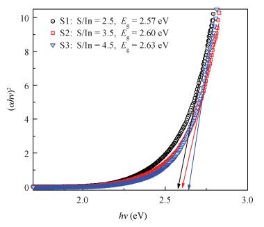
Indium sulfide (In2S3) thin films were prepared by chemical spray pyrolysis technique from solutions with different[S]/[In] ratios on glass substrates at a constant temperature of 250℃. Thin films were characterized by X-ray diffraction (XRD), scanning electron microscopy (SEM), atomic force microscopy (AFM), energy dispersive X-ray spectroscopy (EDS), Raman spectroscopy and optical transmittance spectroscopy. All samples exhibit a polycrystalline structure with a preferential orientation along (0, 0, 12). A good stoichiometry was attained for all samples. The morphology of thin film surfaces, as seen by SEM, was dense and no cracks or pinholes were observed. Raman spectroscopy analysis shows active modes belonging to β-ln2S3 phase. The optical transmittance in the visible range is higher than 60% and the band gap energy slightly increases with the sulfur to indium ratio, attaining a value of 2.63 eV for[S]/[In]=4.5.


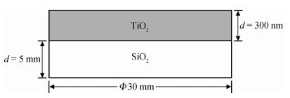
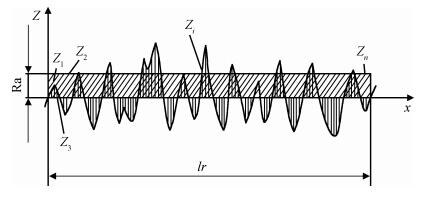
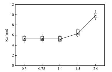
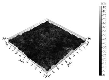
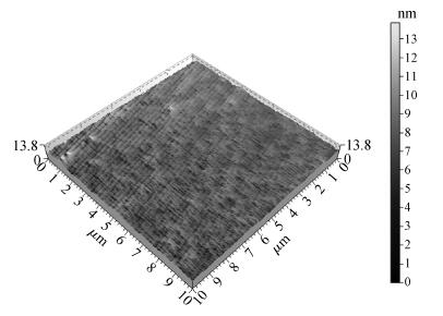
Surface roughness by peaks and depressions on the surface of titanium dioxide (TiO2) thin film, which was widely used for an antireflection coating of optical systems, caused the extinction coefficient increase and affected the properties of optical system. Chemical mechanical polishing (CMP) is a very important method for surface smoothing. In this polishing experiment, we used self-formulated weakly alkaline slurry. Other process parameters were working pressure, slurry flow rate, head speed, and platen speed. In order to get the best surface roughness (1.16 Å, the scanned area was 10×10 μm2) and a higher polishing rate (60.8 nm/min), the optimal parameters were:pressure, 1 psi; slurry flow rate, 250 mL/min; polishing head speed, 80 rpm; platen speed, 87 rpm.


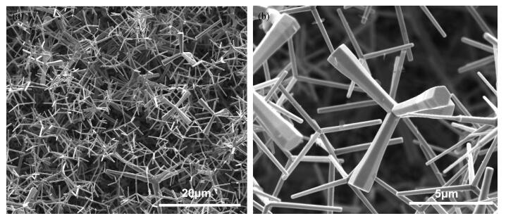
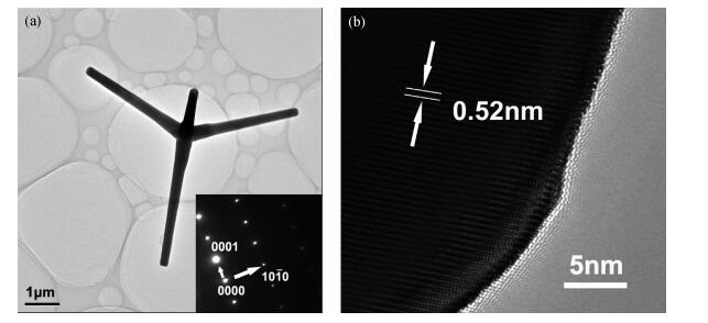
The tetrapod ZnO nanostructures are synthesized on the Si (100) substrates using the chemical vapor deposition (CVD) method at 1000℃. Each nanostructure has four arms which are about 3-10 μm in length and 0.2-1.5 μm in diameter. Further analyses on structure demonstrate that the tetrapod ZnO nanostructures have single crystalline wurtzite hexagonal structure preferentially oriented in c-axis. The photoluminescence (PL) measurements of the tetrapod ZnO nanostructures revealed a UV peak at 382 nm corresponding to the free exciton emission, and a green peak at 523 nm arising from deep level emission. For comparative analysis, cathodoluminescence (CL) spectra obtained from different regions of an individual tetrapod are investigated. Moreover, a possible growth mechanism of the tetrapod ZnO nanostructures is also discussed based on the experimental results.


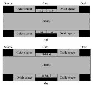
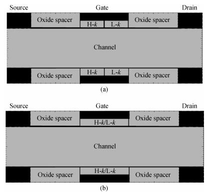
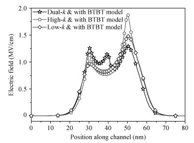
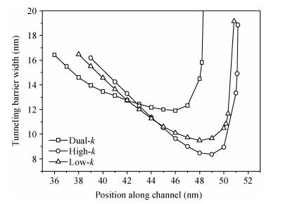
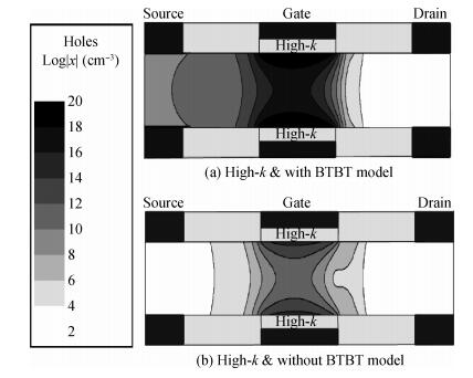
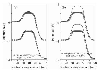
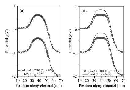
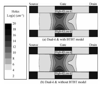
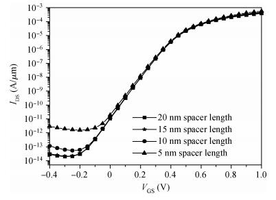
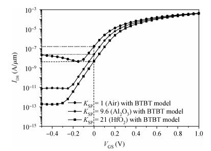
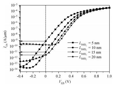
We propose a hetero-gate-dielectric double gate junctionless transistor (HGJLT), taking high-k gate insulator at source side and low-k gate insulator at drain side, which reduces the effects of band-to-band tunnelling (BTBT) in the sub-threshold region. A junctionless transistor (JLT) is turned off by the depletion of carriers in the highly doped thin channel (device layer) which results in a significant band overlap between the valence band of the channel region and the conduction band of the drain region, due to off-state drain bias, that triggers electrons to tunnel from the valence band of the channel region to the conduction band of the drain region leaving behind holes in the channel.These effects of band-to-band tunnelling increase the sub-threshold leakage current, and the accumulation of holes in the channel forms a parasitic bipolar junction transistor (n-p-n BJT for channel JLT) in the lateral direction by the source (emitter), channel (base) and drain (collector) regions in JLT structure in off-state. The proposed HGJLT reduces the subthreshold leakage current and suppresses the parasitic BJT action in off-state by reducing the band-to-band tunnelling probability.


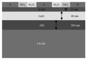
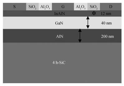
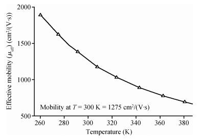
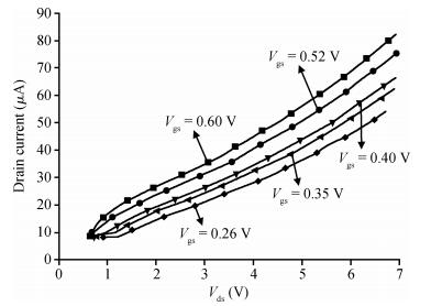
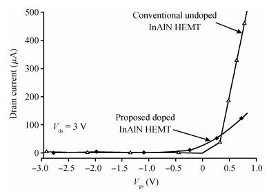
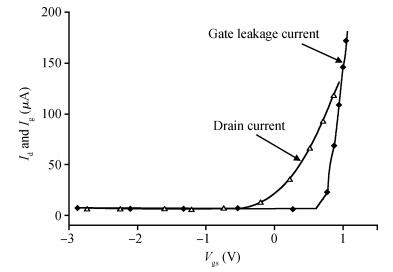
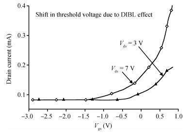
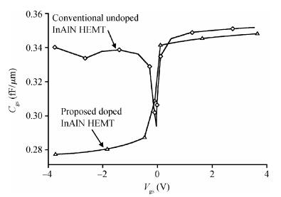
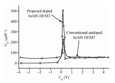
We propose a new structure of InxAl1-xN/GaN high electron mobility transistor (HEMT) with gate length of 20 nm. The threshold voltage of this HEMT is achieved as -0.472 V. In this device the InAlN barrier layer is intentionally n-doped to boost the ION/IOFF ratio. The InAlN layer acts as donor barrier layer for this HEMT which exhibits an ION=10-4.3 A and a very low IOFF=10-14.4 A resulting in an ION/IOFF ratio of 1010.1. We compared our obtained results with the conventional InAlN/GaN HEMT device having undoped barrier and found that the proposed device has almost 105 times better ION/IOFF ratio. Further, the mobility analysis in GaN channel of this proposed HEMT structure along with DC analysis, C-V and conductance characteristics by using small-signal analysis are also presented in this paper. Moreover, the shifts in threshold voltage by DIBL effect and gate leakage current in the proposed HEMT are also discussed. InAlN was chosen as the most preferred barrier layer as a replacement of AlGaN for its excellent thermal conductivity and very good scalability.


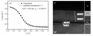
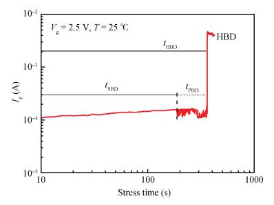
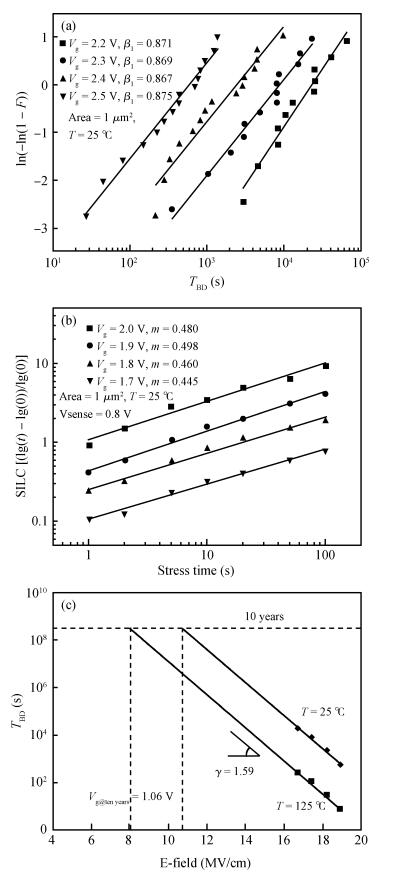
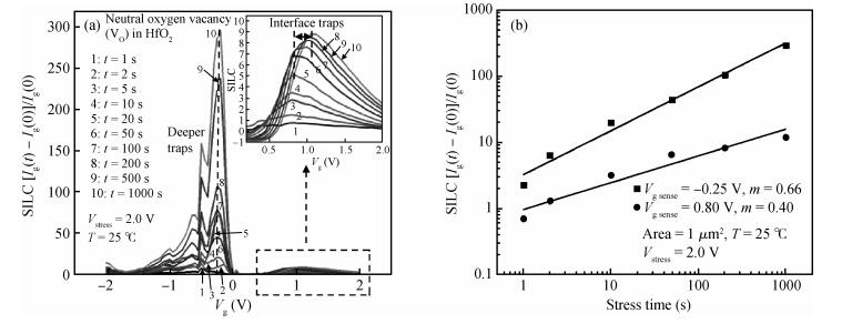
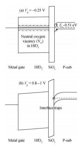
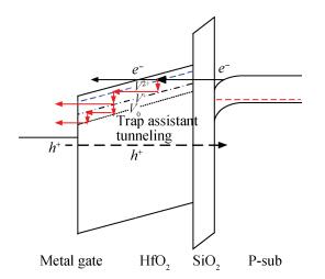
The characteristics of TDDB (time-dependent dielectric breakdown) and SILC (stress-induced leakage current) for an ultra-thin SiO2/HfO2 gate dielectric stack are studied. The EOT (equivalent-oxide-thickness) of the gate stack (Si/SiO2/HfO2/TiN/TiAl/TiN/W) is 0.91 nm. The field acceleration factor (γ) extracted in TDDB experiments is 1.59 s·cm/MV, and the maximum voltage is 1.06 V when the devices operate at 125℃ for ten years. A detailed study on the defect generation mechanism induced by SILC is presented to deeply understand the breakdown behavior. The trap energy levels can be calculated by the SILC peaks:one SILC peak is most likely to be caused by the neutral oxygen vacancy (VO) in the HfO2 bulk layer at 0.51 eV below the Si conduction band minimum; another SILC peak is induced by the interface traps, which are aligned with the silicon conduction band edge. Furthermore, the great difference between the two SILC peaks demonstrates that the degeneration of the high-k layer dominates the breakdown behavior of the extremely thin gate dielectric.


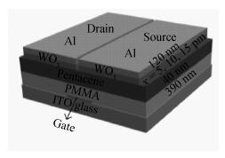
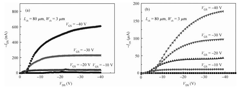
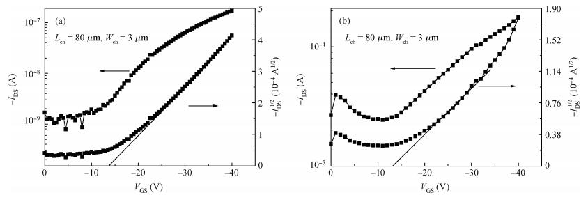
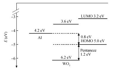
The pentacene-based organic field effect transistor (OFET) with a thin transition metal oxide (WO3) layer between pentacene and metal (Al) source/drain electrodes was fabricated. Compared with conventional OFET with only metal Al source/drain electrodes, the introduction of the WO3 buffer layer leads to the device performance enhancement. The effective field-effect mobility and threshold voltage are improved to 1.90 cm2/(V·s) and 13 V, respectively. The performance improvements are attributed to the decrease of the interface energy barrier and the contact resistance. The results indicate that it is an effective approach to improve the OFET performance by using a WO3 buffer layer.


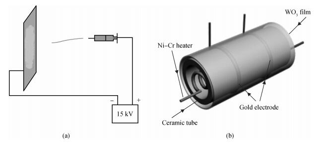
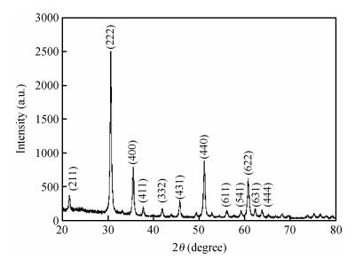
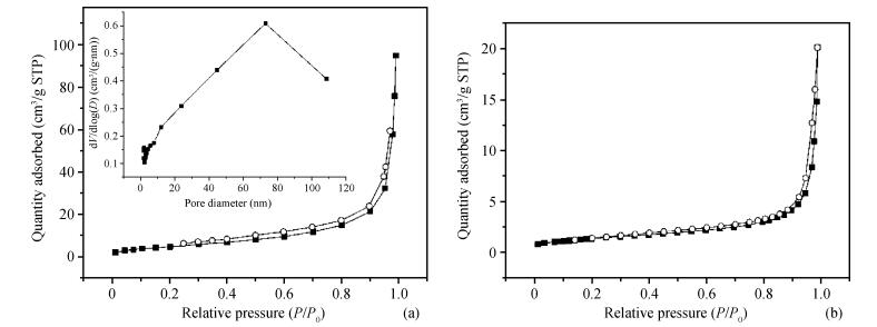
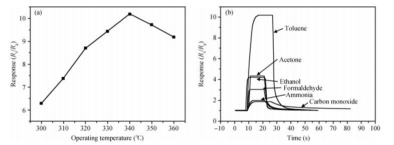
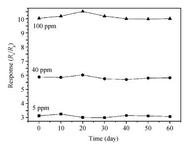
The pristine In2O3 nanotubes were synthesized by electrospinning and subsequent calcination. Scanning electron microscope, X-ray powder diffraction and transmission electron micrograph were employed to analyze the morphology and crystal structure of the as-synthesized nanotubes. Gas-sensing properties of the as-synthesized In2O3 nanotubes were investigated by exposing the corresponding sensors to toluene, acetone, ethanol, formaldehyde, ammonia and carbon monoxide at 340℃. The results show that the gas sensor possesses a good selectivity to toluene at 340℃. The response of the In2O3 nanotube gas sensor to 40 ppm is about 5.88. The response and recovery times are about 3 s and 17 s, respectively.


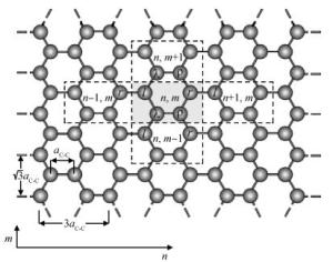
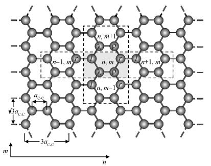
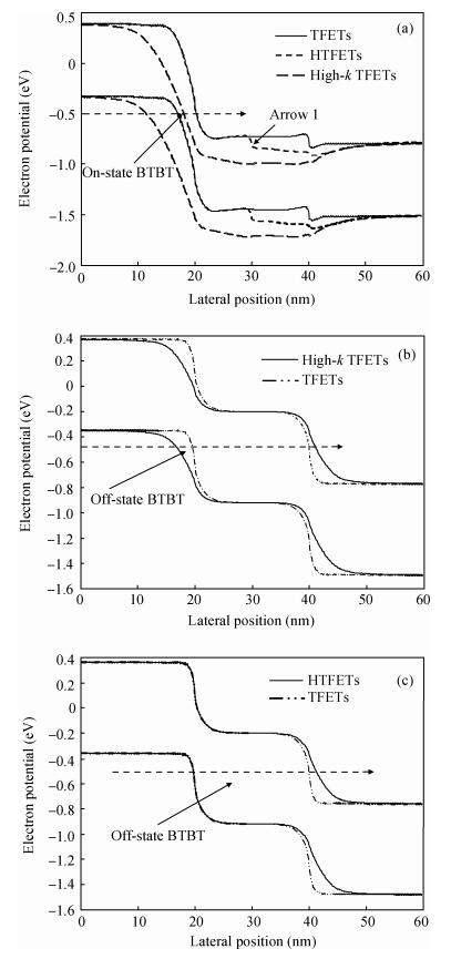
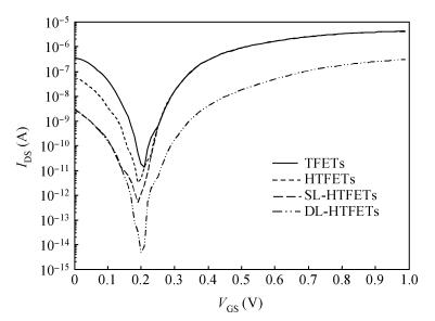
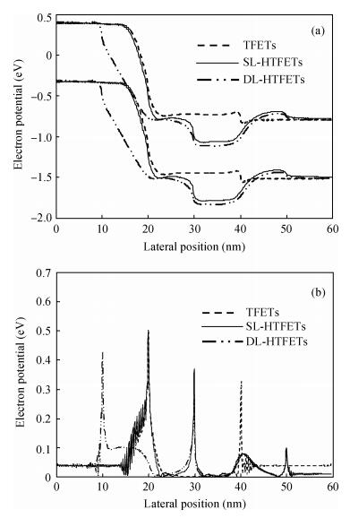
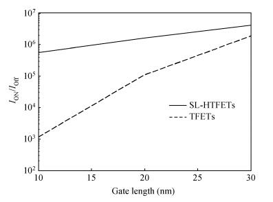
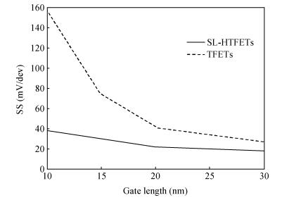
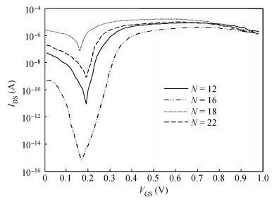
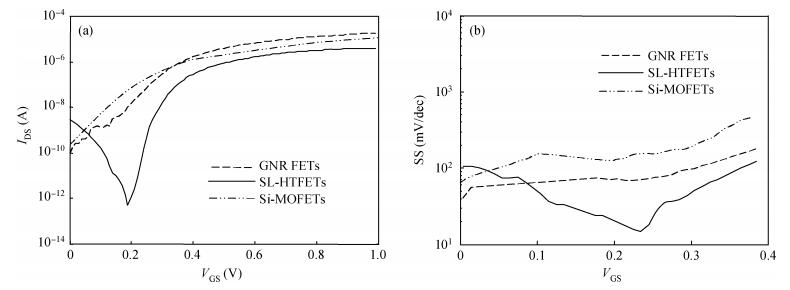
We perform a theoretical study of the effects of the lightly doped drain (LDD) and high-k dielectric on the performances of double gate p-i-n tunneling graphene nanoribbon field effect transistors (TFETs). The models are based on non-equilibrium Green's functions (NEGF) solved self-consistently with 3D-Poisson's equations. For the first time, hetero gate dielectric and single LDD TFETs (SL-HTFETs) are proposed and investigated. Simulation results show SL-HTFETs can effectively decrease leakage current, sub-threshold swing, and increase on-off current ratio compared to conventional TFETs and Si-based devices; the SL-HTFETs from the 3p + 1 family have better switching characteristics than those from the 3p family due to smaller effective masses of the former. In addition, comparison of scaled performances between SL-HTFETs and conventional TFETs show that SL-HTFETs have better scaling properties than the conventional TFETs, and thus could be promising devices for logic and ultra-low power applications.


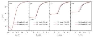
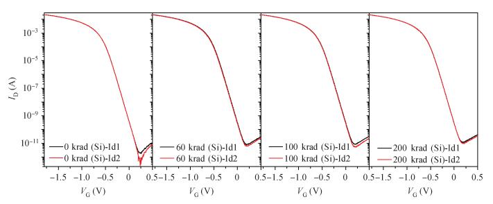
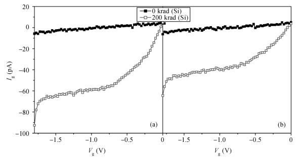
Based on 0.18 μm MOS transistors, for the first time, the total dose effects on the matching properties of deep submicron MOS transistors are studied. The experimental results show that the total dose radiation magnifies the mismatch among identically designed MOS transistors. In our experiments, as the radiation total dose rises to 200 krad, the threshold voltage and drain current mismatch percentages of NMOS transistors increase from 0.55% and 1.4% before radiation to 17.4% and 13.5% after radiation, respectively. PMOS transistors seem to be resistant to radiation damage. For all the range of radiation total dose, the threshold voltage and drain current mismatch percentages of PMOS transistors keep under 0.5% and 2.72%, respectively.


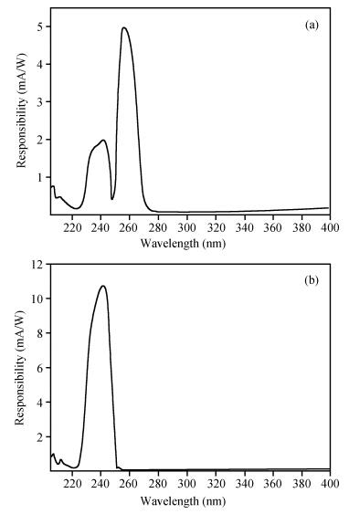
Back-illuminated AlxGa1-xN-based dual-band solar-blind ultraviolet (UV) photodetectors (PDs) are realized by a three-terminal n-i-p-i-n heterojunction structure which is grown on sapphire substrate by metal organic chemical vapor deposition (MOCVD). The two p-i-n junctions contained in the heterojunction structure can work separately and independently. Working in the photovoltaic mode, the PDs display peak responsivity of~10.8 mA/W at 242 nm and~5.0 mA/W at 257 nm, respectively. The two junctions with different size, whose diameters are 500 μm and 800 μm, exhibit almost the same leakage current of~1.3×10⁻⁹ A at a reverse bias of 10 V. Therefore, dark current densities of the two junctions are close to 6.6×10⁻⁷ A/cm2 and 2.6×10⁻⁷ A/cm2 at -10 V respectively.


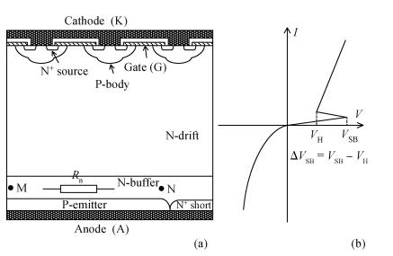
A physically based equation for predicting required p-emitter length of a snapback-free reverse-conducting insulated gate bipolar transistor (RC-IGBT) with field-stop structure is proposed. The n-buffer resistances above the p-emitter region with anode geometries of linear strip, circular and annular type are calculated, and based on this, the minimum p-emitter lengths of those three geometries are given and verified by simulation. It is found that good agreement was achieved between the numerical calculation and simulation results. Moreover, the calculation results show that the annular case needs the shortest p-emitter length for RC-IGBT to be snapback-free.


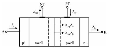
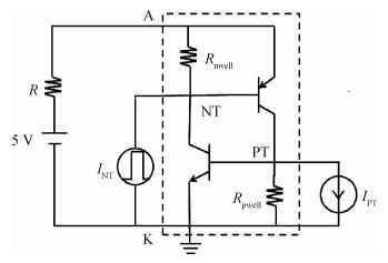
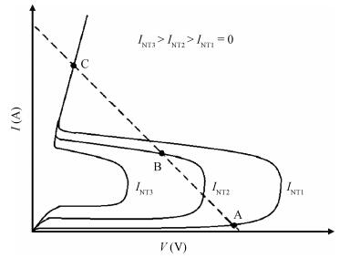
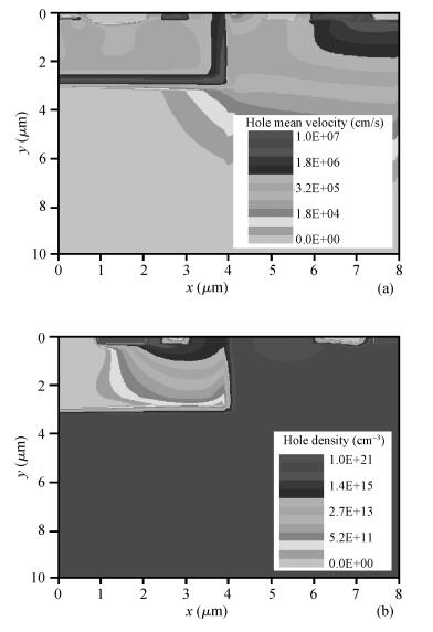
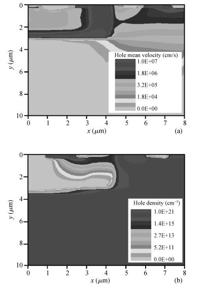
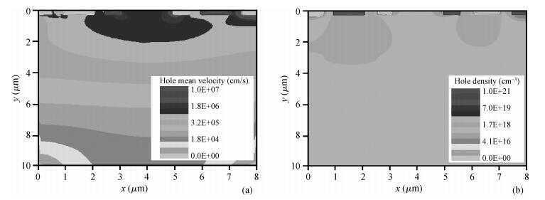
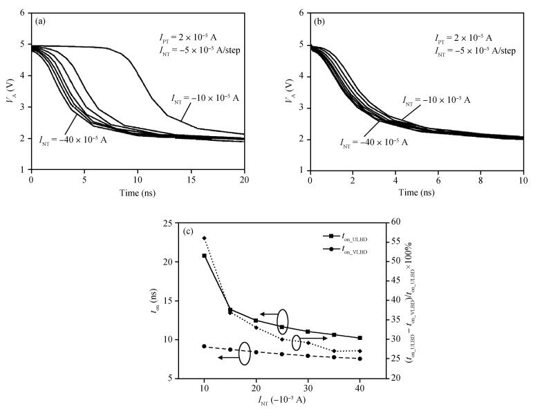
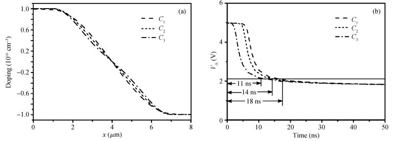
The turn-on speed of electrostatic discharge (ESD) protection devices is very important for the protection of the ultrathin gate oxide. A double trigger silicon controlled rectifier device (DTSCR) can be used effectively for ESD protection because it can turn on relatively quickly. The turn-on process of the DTSCR is first studied, and a formula for calculating the turn-on time of the DTSCR is derived. It is found that the turn-on time of the DTSCR is determined mainly by the base transit time of the parasitic p-n-p and n-p-n transistors. Using the variation lateral base doping (VLBD) structure can reduce the base transit time, and a novel DTSCR device with a VLBD structure (VLBD_DTSCR) is proposed for ESD protection applications. The static-state and turn-on characteristics of the VLBD_DTSCR device are simulated. The simulation results show that the VLBD structure can introduce a built-in electric field in the base region of the parasitic n-p-n and p-n-p bipolar transistors to accelerate the transport of free-carriers through the base region. In the same process and layout area, the turn-on time of the VLBD_DTSCR device is at least 27% less than that of the DTSCR device with the traditional uniform base doping under the same value of the trigger current.


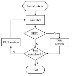
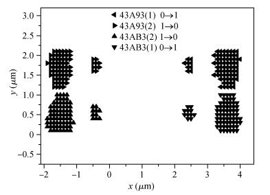
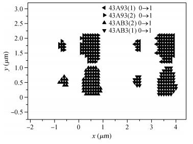
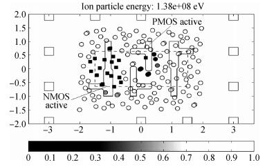
The pulsed laser facility for SEU sensitivity mapping is utilized to study the SEU sensitive regions of a 0.18 μm CMOS SRAM cell. Combined with the device layout micrograph, SEU sensitivity maps of the SRAM cell are obtained. TCAD simulation work is performed to examine the SEU sensitivity characteristics of the SRAM cell. The laser mapping experiment results are discussed and compared with the electron micrograph information of the SRAM cell and the TCAD simulation results. The results present that the test technique is reliable and of high mapping precision for the deep submicron technology device.


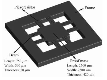
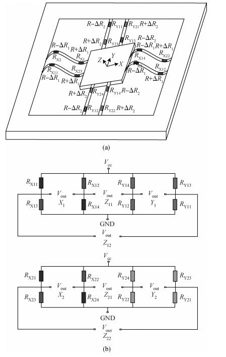
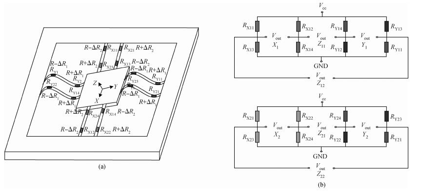
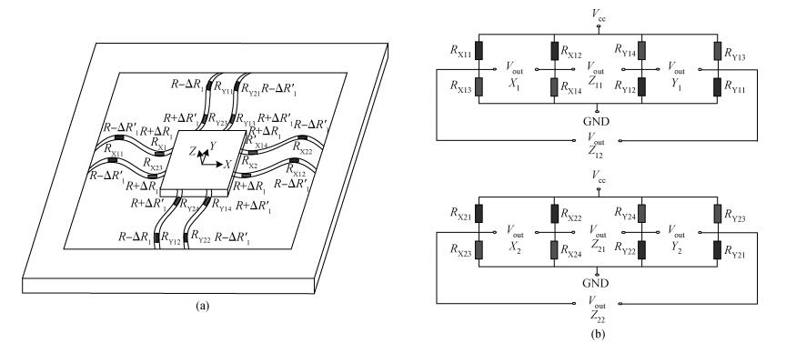
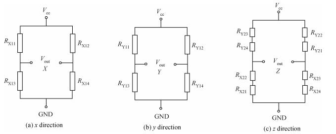
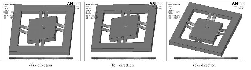
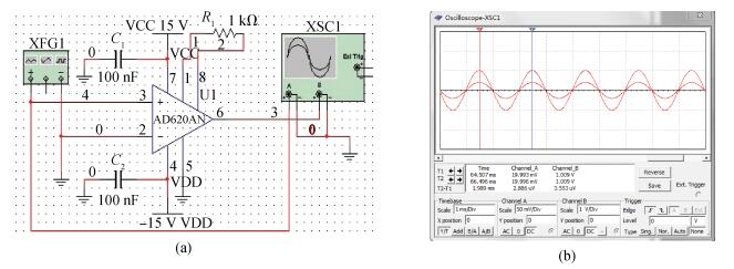
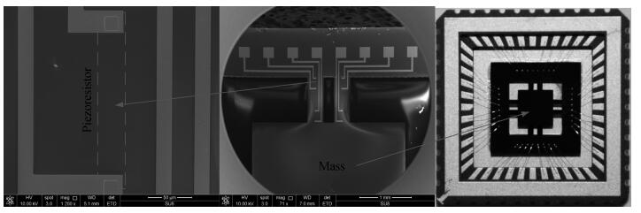
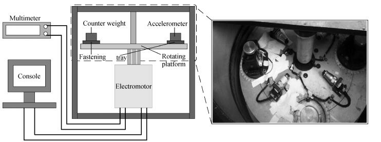
A cycle bridge detection method, which uses a piezoresistive triaxial accelerometer, has been described innovatively. This method just uses eight resistors to form a cycle detection bridge, which can detect the signal of the three directions for real time. It breaks the law of the ordinary independent Wheatstone bridge detection method, which uses at least 12 resistors and each four resistors connected as a Wheatstone bridge to detect the output signal from a specific direction. In order to verify the feasibility of this method, the modeling and simulating of the sensor structure have been conducted by ANSYS, then the dual cycle bridge detection method and independent Wheatstone bridge detection method are compared, the result shows that the former method can improve the sensitivity of the sensor effectively. The sensitivity of the x, y-axis used in the former method is two times that of the sensor used in the latter method, and the sensitivity of the z-axis is four times. At the same time, it can also reduce the cross-axis coupling degree of the sensor used in the dual cycle bridge detection method. In addition, a signal amplifier circuit and adder circuit have been provided. Finally, the test result of the "eight-beams/mass" triaxial accelerometer, which is based on the dual cycle bridge detection method and the related circuits, have been provided. The results of the test and the theoretical analysis are consistent, on the whole.


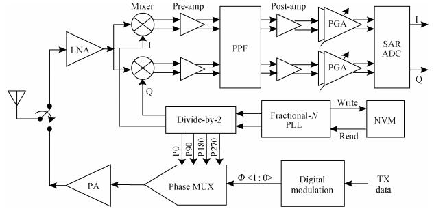
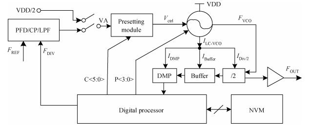
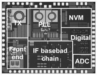
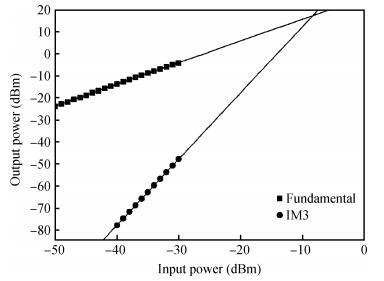
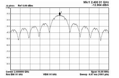
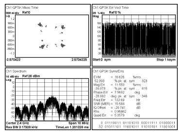
This paper presents a 2.4 GHz CMOS transceiver for the wireless personal area network (WPAN) integrated in 0.18 μm CMOS technology. This transceiver adopts a low-IF receiver, a MUX based transmitter and a fast-setting fractional-N frequency synthesizer. For achieving low cost and low power consumption, an inductor-less receiver front-end, an adaptive analog baseband, a low power MUX and a current-reused phase-locked loop (PLL) have been proposed in this work. Measured results show that the receiver achieves -8 dBm of ⅡP3 and 31 dB of image rejection. The transmitter delivers 0 dBm output power at a data rate of 2 Mbps. The current consumption is 7.2 mA in the receiving mode and 6.9 mA in the transmitting mode, respectively.


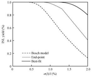
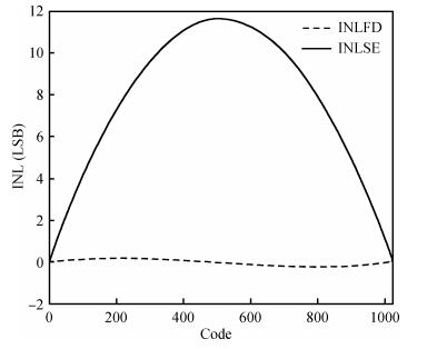
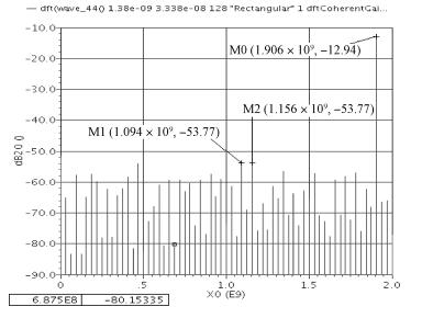
A 10 bit 250 MS/s current-steering digital-to-analog converter is presented. Only standard VT core devices are available for the sake of simplicity and low cost. In order to meet the INL performance, a Monte Carlo model is built to analyze the impact of mismatch on integral nonlinearity (INL) yield with both end-point line and best-fit line. A formula is derived for the relationship of INL and output impedance. The relation of dynamic range and output impedance is also discussed. The double centroid layout is adopted for the current source array in order to mitigate the effect of electrical, process, and temperature gradient. An adapted current mirror is used to overcome the gate leakage of the current source array, which cannot be ignored in the 65 nm GP CMOS process. The digital-to-analog converter occupies 0.06 mm2, and consumes 2.5 mW from a single 1.0 V supply at 250 MS/s.


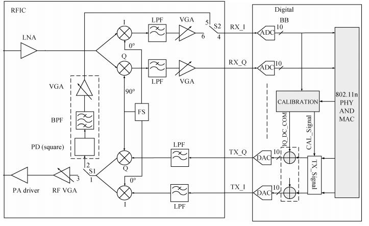
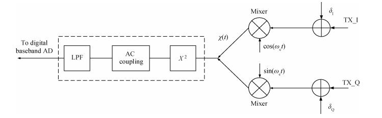
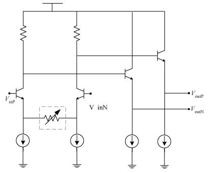
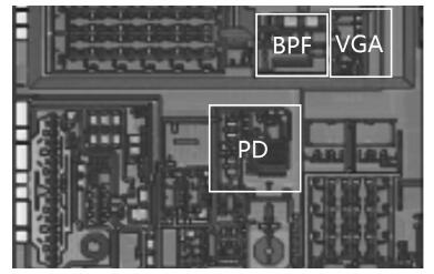
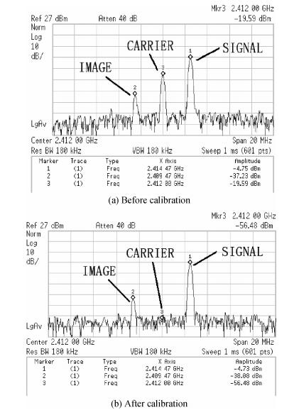
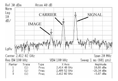
A carrier leakage calibration and compensation technique based on digital baseband for a wideband wireless communication transceiver is proposed. The digital baseband transmits a calibration signal, samples the signal which passes through the transmitter path and the calibration loop in the RF chip, measures the carrier leakage by analyzing the sampled data and compensates it. Compared with a self-calibration technique in the RF chip, the proposed technique saves area and power consumption for the wireless local area network (WLAN) solution. This technique has been successfully used for 802.11n system and satisfies the requirement of the standard by achieving over 50 dB carrier leakage suppression.


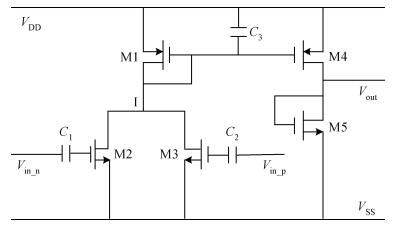


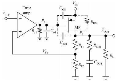
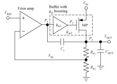
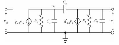
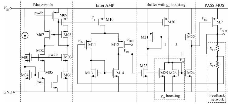
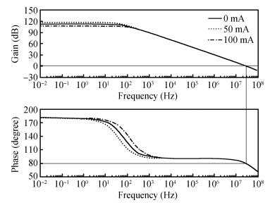
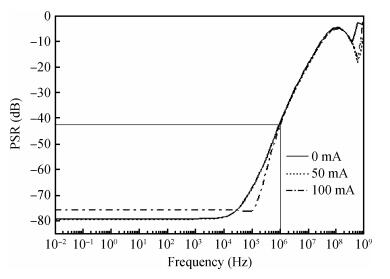
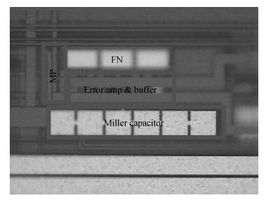
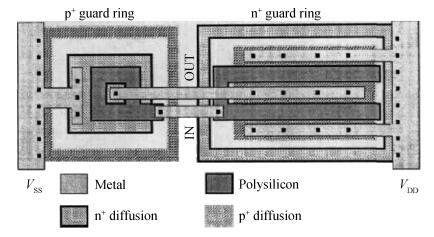
This paper presents a capacitor-free CMOS low dropout voltage regulator which has high PSR performance and low chip area. Pole splitting and gm boosting techniques are employed to achieve good stability. The capacitor-free chip LDO was fabricated in commercial 0.18 μm CMOS technology provided by GSMC (Shanghai, China). Measured results show that the capacitor-free LDO has a stable output voltage 1.79 V, when supply voltage changes from 2.5 to 5 V, and the LDO is capable of driving maximum 100 mA load current. The LDO has high power supply rejection about -79 dB at low frequency and -40 dB at 1 MHz frequency, while sacrifice of the LDO's active chip-area is only smaller than 0.02 mm2.


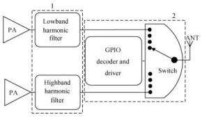
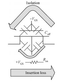
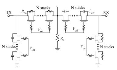
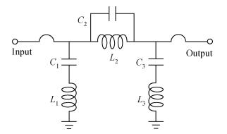
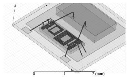
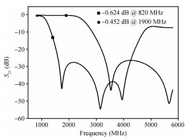
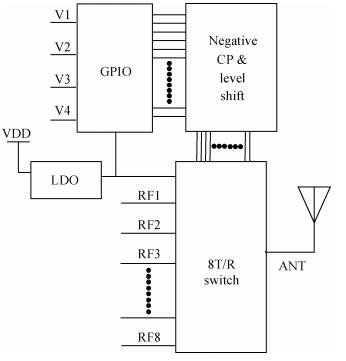
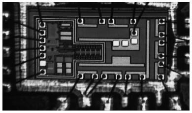
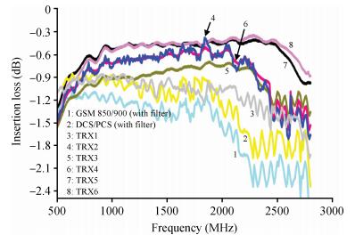
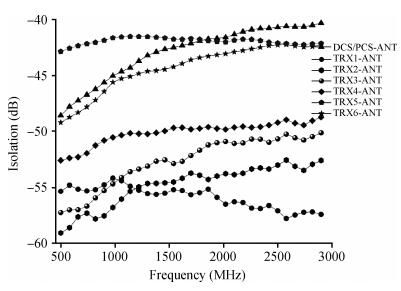
A broadband monolithic linear single pole, eight throw (SP8T) switch has been fabricated in 180 nm thin film silicon-on-insulator (SOI) CMOS technology with a quad-band GSM harmonic filter in integrated passive devices (IPD) technology, which is developed for cellular applications. The antenna switch module (ASM) features 1.2 dB insertion loss with filter on 2G bands and 0.4 dB insertion loss in 3G bands, less than -45 dB isolation and maximum -103 dB intermodulation distortion for mobile front ends by applying distributed architecture and adaptive supply voltage generator.


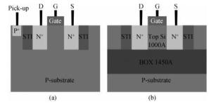
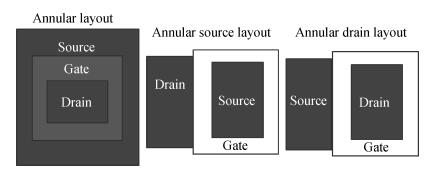
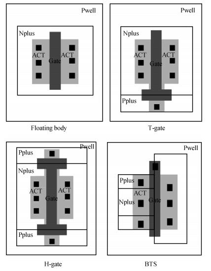
Total ionizing dose (TID) effect and single event effect (SEE) from space may cause serious effects on bulk silicon and silicon on insulator (SOI) devices, so designers must pay much attention to these bad effects to achieve better performance. This paper presents different radiation-hardened layout techniques to mitigate TID and SEE effect on bulk silicon and SOI device and their corresponding advantages and disadvantages are studied in detail. Under 0.13 μm bulk silicon and SOI process technology, performance comparisons of two different kinds of DFF circuit are made, of which one kind is only hardened in layout (protection ring for bulk silicon DFF, T-gate for SOI DFF), while the other kind is also hardened in schematic such as DICE structure. The result shows that static power and leakage of SOI DFF is lower than that of bulk silicon DFF, while SOI DFF with T-gate is a little slower than bulk silicon DFF with protection ring, which will provide useful guidance for radiation-hardened circuit and layout design.


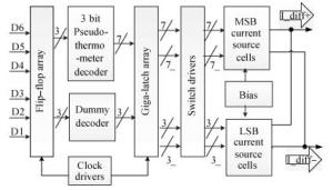
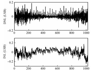
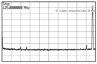
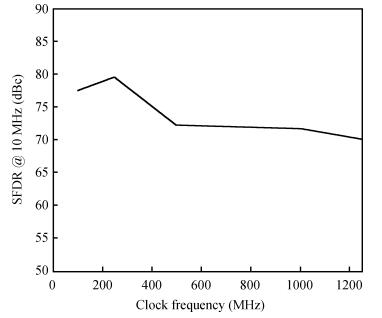
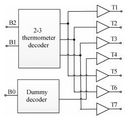
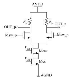
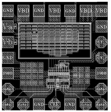
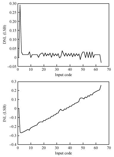
A 6-bit 4 GS/s, high-speed and power-efficient DAC for ultra-high-speed transceivers in 60 GHz band millimeter wave technology is presented. A novel pseudo-thermometer architecture is proposed to realize a good compromise between the fast conversion speed and the chip area. Symmetrical and compact floor planning and layout techniques including tree-like routing, cross-quading and common-centroid method are adopted to guarantee the chip is fully functional up to near-Nyquist frequency in a standard 0.18 μm CMOS process. Post simulation results corroborate the feasibility of the designed DAC, which can perform good static and dynamic linearity without calibration. DNL errors and INL errors can be controlled within ±0.28 LSB and ±0.26 LSB, respectively. SFDR at 4 GHz clock frequency for a 1.9 GHz near-Nyquist sinusoidal output signal is 40.83 dB and the power dissipation is less than 37 mW.


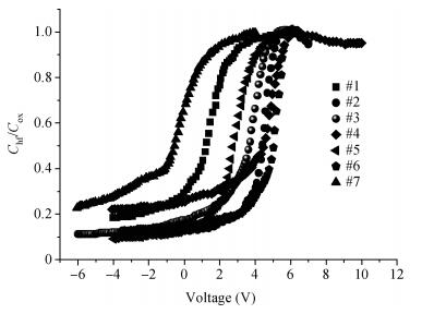
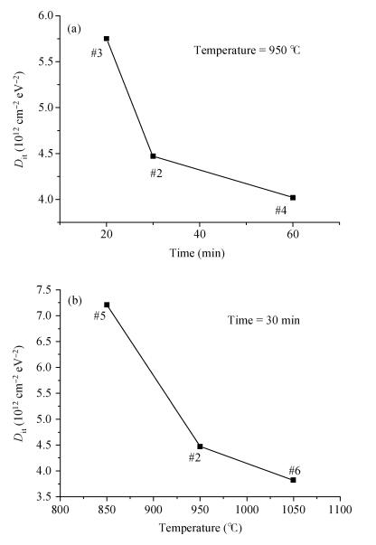
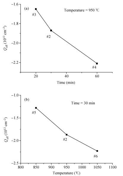
The effect of the different re-oxidation annealing (ROA) processes on the SiO2/SiC interface characteristics has been investigated. With different annealing processes, the flat band voltage, effective dielectric charge density and interface trap density are obtained from the capacitance-voltage curves. It is found that the lowest interface trap density is obtained by the wet-oxidation annealing process at 1050℃ for 30 min, while a large number of effective dielectric charges are generated. The components at the SiO2/SiC interface are analyzed by X-ray photoelectron spectroscopy (XPS) testing. It is found that the effective dielectric charges are generated due to the existence of the C and H atoms in the wet-oxidation annealing process.

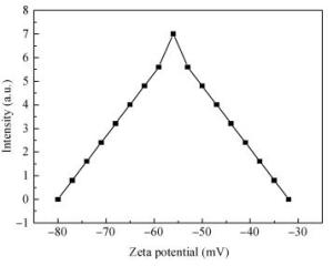
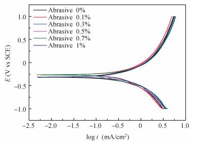
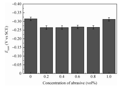
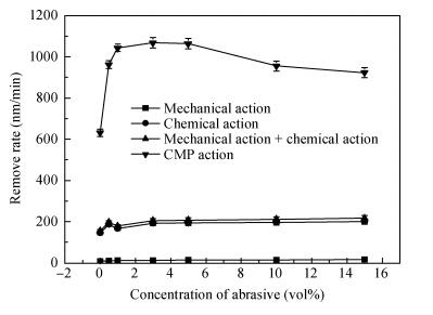
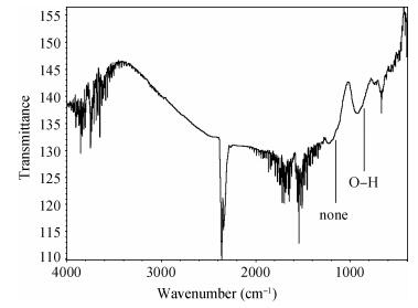
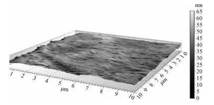
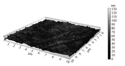
There is a lot of hydroxyl on the surface of nano SiO2 sol used as an abrasive in the chemical mechanical planarization (CMP) process, and the chemical reaction activity of the hydroxyl is very strong due to the nano effect. In addition to providing a mechanical polishing effect, SiO2 sol is also directly involved in the chemical reaction. The stability of SiO2 sol was characterized through particle size distribution, zeta potential, viscosity, surface charge and other parameters in order to ensure that the chemical reaction rate in the CMP process, and the surface state of the copper film after CMP was not affected by the SiO2 sol. Polarization curves and corrosion potential of different concentrations of SiO2 sol showed that trace SiO2 sol can effectively weaken the passivation film thickness. In other words, SiO2 sol accelerated the decomposition rate of passive film. It was confirmed that the SiO2 sol as reactant had been involved in the CMP process of copper film as reactant by the effect of trace SiO2 sol on the removal rate of copper film in the CMP process under different conditions. In the CMP process, a small amount of SiO2 sol can drastically alter the chemical reaction rate of the copper film, therefore, the possibility that Cu/SiO2 as a catalytic system catalytically accelerated the chemical reaction in the CMP process was proposed. According to the van't Hoff isotherm formula and the characteristics of a catalyst which only changes the chemical reaction rate without changing the total reaction standard Gibbs free energy, factors affecting the Cu/SiO2 catalytic reaction were derived from the decomposition rate of Cu (OH)2 and the pH value of the system, and then it was concluded that the CuSiO3 as intermediates of Cu/SiO2 catalytic reaction accelerated the chemical reaction rate in the CMP process. It was confirmed that the Cu/SiO2 catalytic system generated the intermediate of the catalytic reaction (CuSiO3) in the CMP process through the removal rate of copper film, infrared spectrum and AFM diagrams in different pH conditions. Finally it is concluded that the SiO2 sol used in the experiment possesses stable performance; in the CMP process it is directly involved in the chemical reaction by creating the intermediate of the catalytic reaction (CuSiO3) whose yield is proportional to the pH value, which accelerates the removal of copper film.