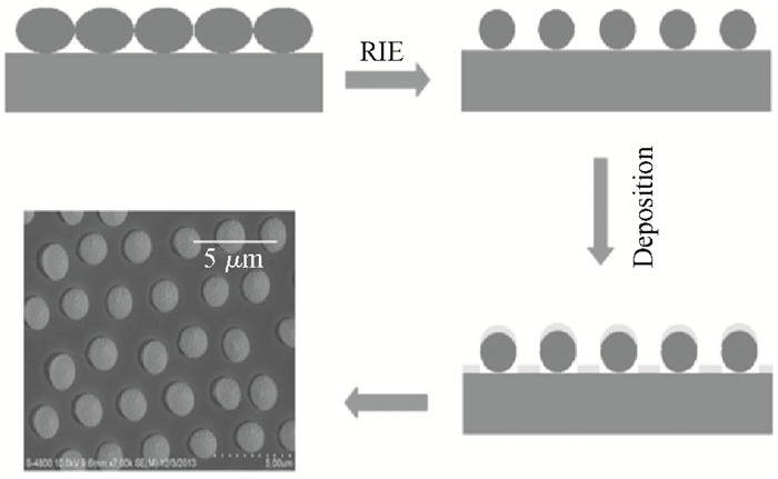
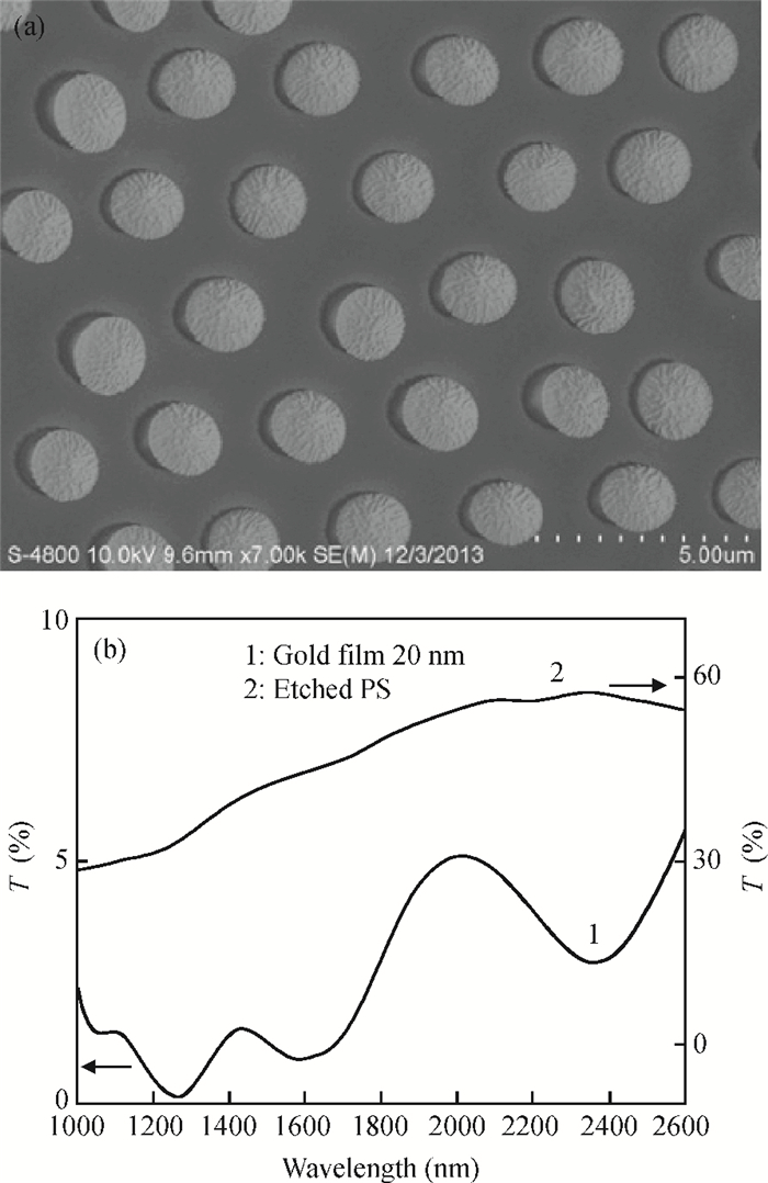
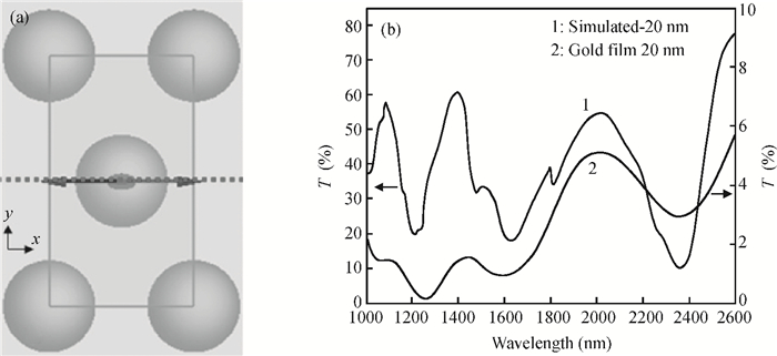
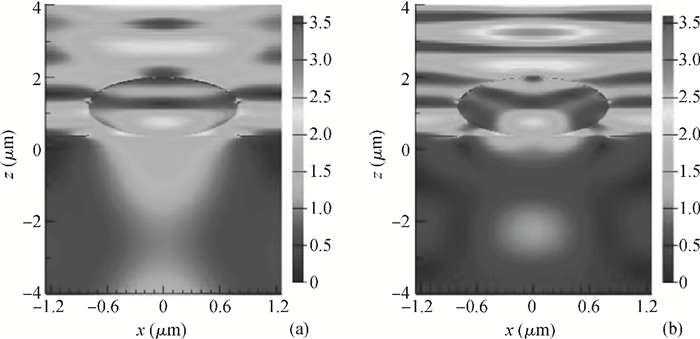
We studied the infrared transmission properties of gold films on ordered two-dimensional non-close-packed polystyrene (PS) colloidal crystal. The gold films consist of gold half-shells on the PS spheres and gold film with 2D arrays of holes on the glass substrate. An extraordinary optical transmission phenomenon could be found in such a structure. Simulations with the finite-difference time-domain method were also employed to get the transmission spectra and electric field distribution. The transmission response of the samples can be adjusted by controlling the thickness of the gold films. Angle-resolved measurements were performed using polarized light to obtain more information about the surface plasmon polariton resonances of the gold films. As the angle changes, the transmission spectra change a lot. The transmission spectra of p-polarized light have quite different properties compared to those of s-polarized light.


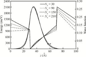
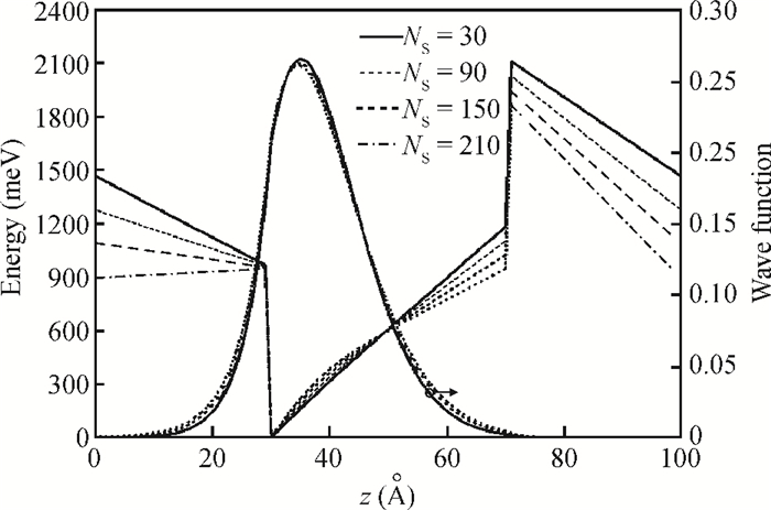
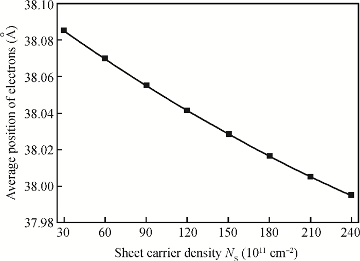
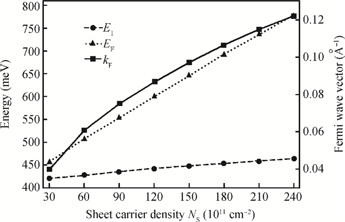
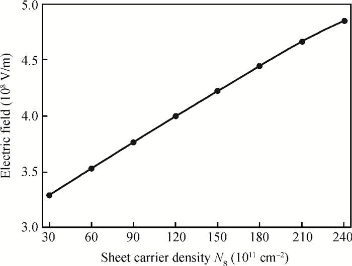
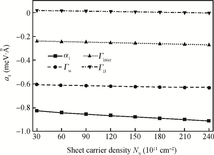
The Rashba coefficient and Rashba spin splitting for the first subband of the Al0.5Ga0.5N/GaN/Al0.5Ga0.5N quantum well (QW) with various sheet carrier densities (Ns) are calculated by solving Schrödinger and Poisson equations self-consistently. The Rashba spin splitting for the first subband at the Fermi level is considerable and increases evidently with Ns, since the Rashba coefficient, especially the Fermi wave vector increase rapidly. With increasing Ns, the peak of the wave function for the first subband moves towards the left heterointerface, and the average electric field in the well increases, so the two dominant contributions coming from the well and the heterointerface increase. Therefore, the strong polarization electric field and high density of 2DEG in ó-nitrides heterostructures are of great importance to ǁ and make the Rashba spin splitting in AlGaN/GaN QWs comparable to that of narrow-gap Ⅲ-Ⅴ materials. The results indicate that the sheet carrier density is an important parameter affecting the Rashba coefficient and Rashba spin splitting in AlGaN/GaN QWs, showing the possible application of this material system in spintronic devices.

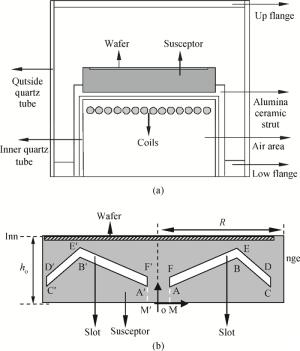
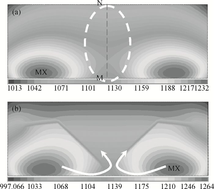
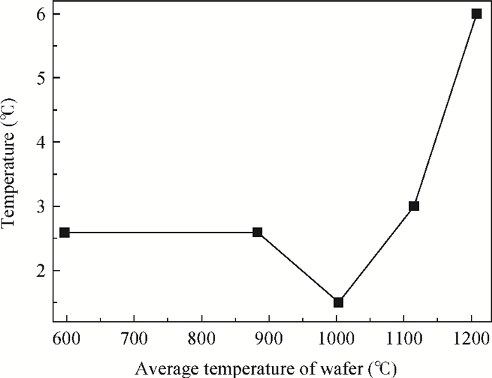
By using the numerical simulation for the temperature field in the metal organic vapor deposition (MOCVD) reactor by induction heating, it is found that the temperature distribution in the conventional cylinder-shaped susceptor is nonuniform due to the skin effect of the induced current, which makes the temperature distribution of the wafer nonuniform. Therefore, a novel susceptor with a ⊥-shaped slot is proposed. This slot changes the mode and the rate of the heat transfer in the susceptor, which improves the uniformity of the temperature distribution in the wafer. By using the finite element method (FEM), the susceptor with this structure for heating a wafer of four inches in diameter is optimized. It is observed that the optimized susceptor with the ⊥-shaped slot makes the uniformity of the temperature distribution in the wafer improve by more than 85%, and a good uniformity of temperature distributions is kept under different wafer temperatures, which may be beneficial to the film growth.


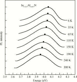
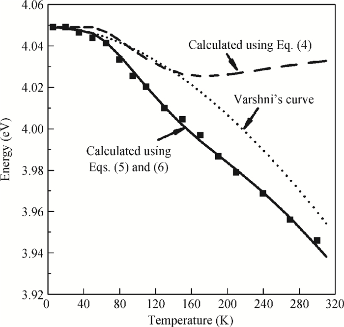
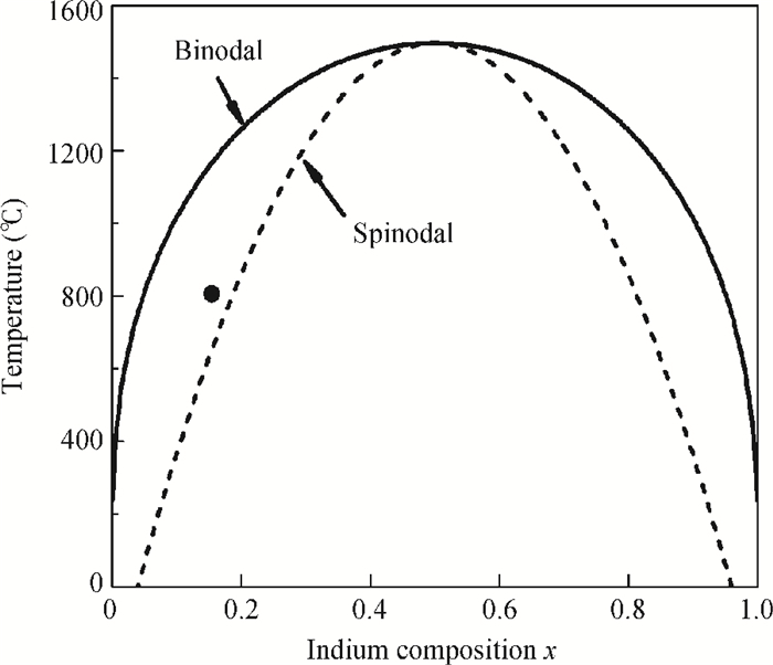
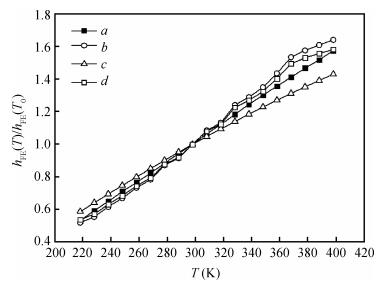
InAlN has been studied by means of temperature-dependent time-integrated photoluminescence and time-resolved photoluminescence. The variation of PL peak energy did not follow the behavior predicted by Varshni formula, and a faster redshift with increasing temperature was observed. We used a model that took account of the thermal activation and thermal transfer of localized excitons to describe and explain the observed behavior. A good fitting to the experiment result is obtained. We believe the anomalous temperature dependence of PL peak energy shift can be attributed to the temperature-dependent redistribution of localized excitons induced by thermal activation and thermal transfer in the strongly localized states. V-shaped defects are thought to be a major factor causing the strong localized states in our In0.153Al0.847N sample.


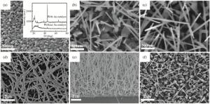
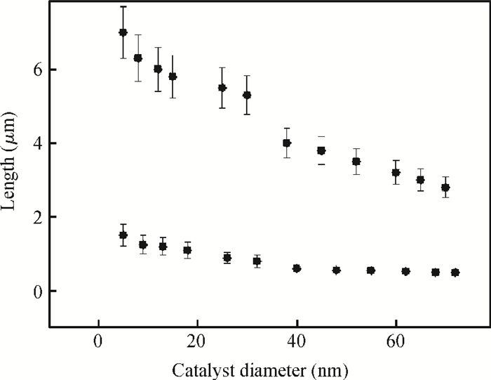
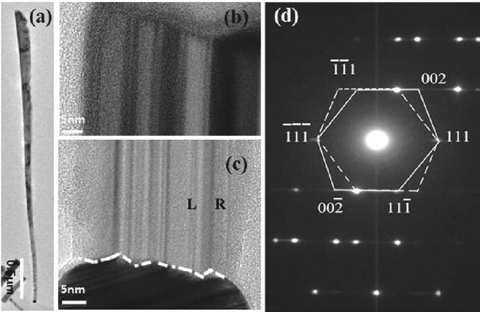
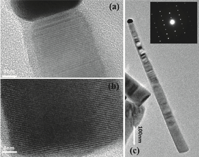
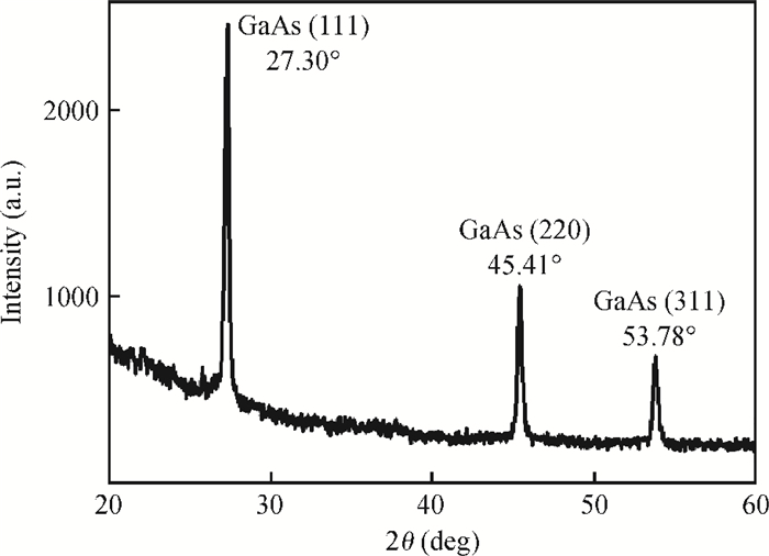
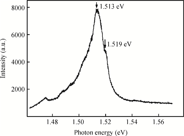
The growth of GaAs nanowires directly on fused quartz substrates using molecular beam epitaxy via a vapor-liquid-solid mechanism with gold as catalyst is reported. Unlike conventional Au-catalyst MBE growth of nanowires (NWs) on GaAs substrates, zinc blende is found to be the dominant crystal structure for NWs grown on fused-quartz substrates by MBE. Further transmission electron microscopy measurements show that the prepared ZB NWs have the growth direction of $[11\overline 2]$ and lamellar {111} twins extend through the length of NWs. Although there are longitudinal planar defects that extend through NWs, the narrow full width at half maximum of PL implies high crystal quality of NWs grown on fused-quartz substrates.

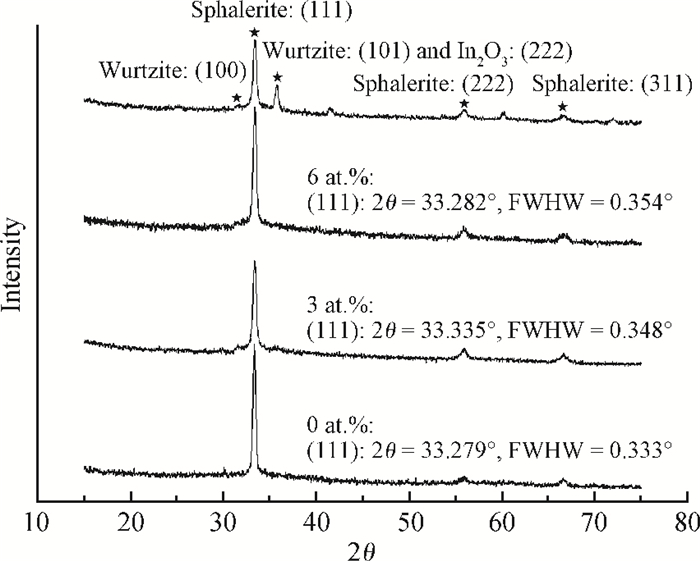
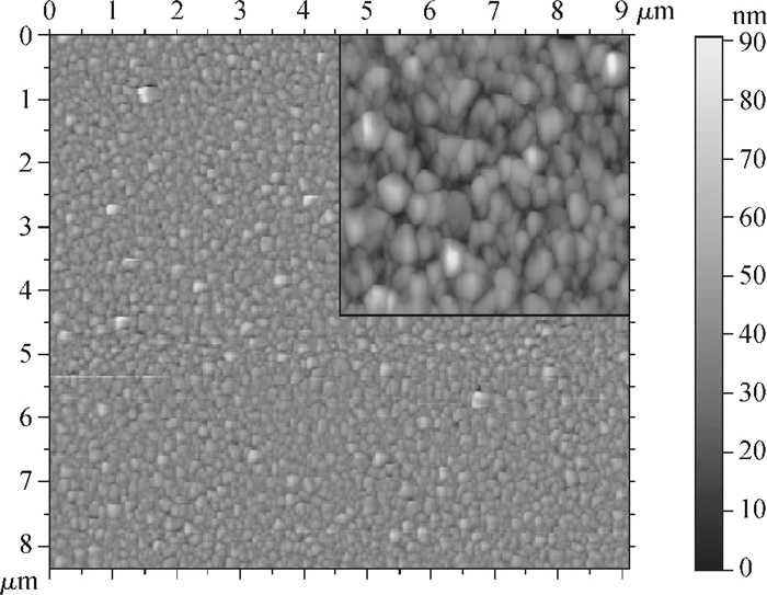
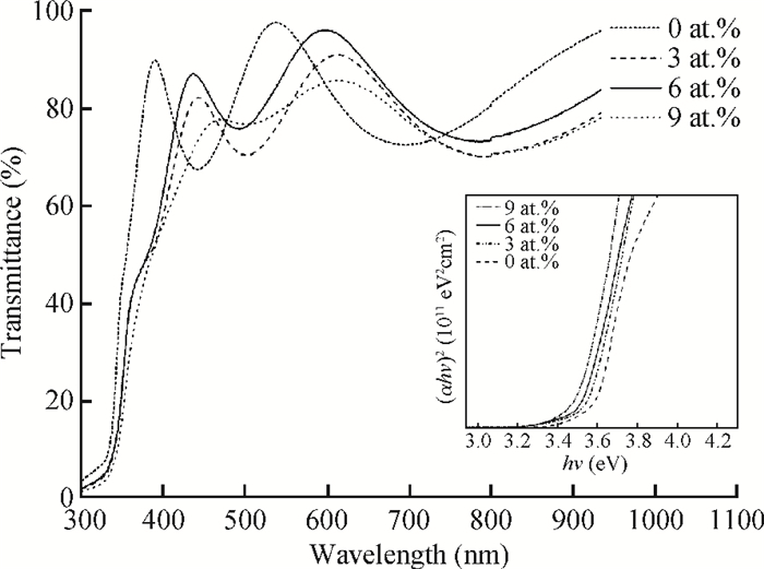
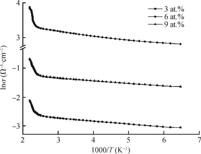
This paper reports a new material, indium-doped ZnS (ZnS:In) film, which is fabricated for the first time to improve its electrical and optical performance. By electron beam evaporation technology and the optimized annealing treatment, high quality ZnS:In film is prepared. XRD indicates that the incorporation of 6 at.% indium atoms into ZnS film causes little lattice deformation. The AFM results imply that large sized particles are compactly dispersed in the ZnS:In layer and results in an unsmooth surface. Electrical and optical property tests show that the resistivity of ZnS film is greatly decreased to 4.46×10⁻² Ω·cm and the optical transmittance is improved to 85% in the visible region. Comparing with the results in other literatures, significant progress in electrical/optical performance has been made in this paper.
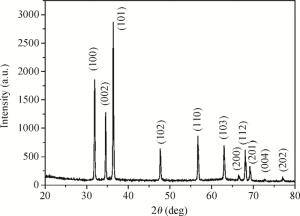
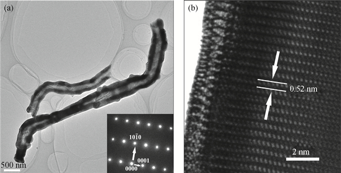
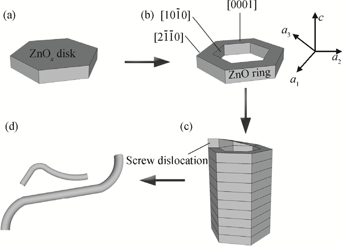
ZnO nanotubes have been fabricated through a carbon thermal reduction deposition process. Structure characterization results show that the ZnO nanotubes have a single crystalline wurtzite hexagonal structure preferentially oriented in the c-axis. The diameters of ZnO nanotubes are in the range of 90-280 nm and the wall thickness is about 50-100 nm. Room-temperature photoluminescence measurements of the ZnO nanotubes exhibit an intensive ultraviolet peak at 377 nm and a broad peak centered at about 517 nm. The UV emission is caused by the near band edge emission while the green emission may be attributed to both oxygen vacancy and the surface state. Raman and cathodoluminescence spectra are also discussed. Finally, a possible growth mechanism of the ZnO nanotubes is proposed.


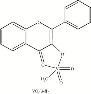
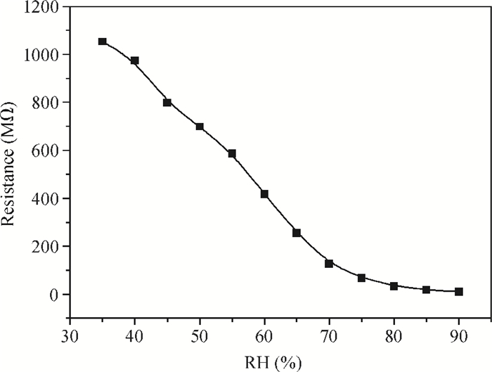
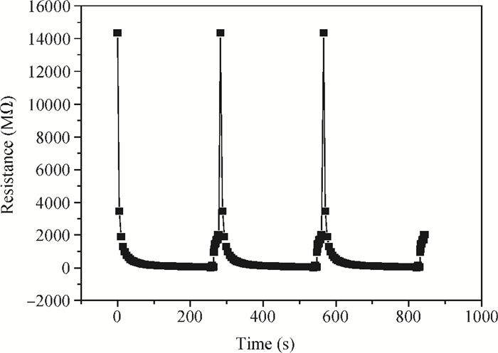
A resistive-type relative humidity (RH) sensor based on vanadium complex (VO2(3-fl)) film is reported in this study. Gold electrodes were deposited on the glass substrates in a co-planar structure. A thin film of vanadium complex was coated as a humidity-sensing material on the top of the pre-patterned electrodes. The humidity-sensing principle of the sensor was based on the conductivity change of coated sensing element upon adsorption/desorption of water vapor. The resistance of the humidity sensor measured at 1 kHz decreased linearly with increasing the humidity in the range of 35%-70% RH. The overall resistance of the sensor decreases 11 times. An equivalent circuit for the VO2(3-fl) based resistive-type humidity sensor was developed. The properties of the sensor studied in this work make it beneficial for use in the instruments for environmental monitoring of humidity.


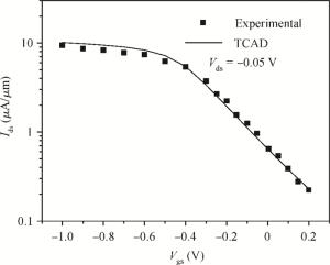
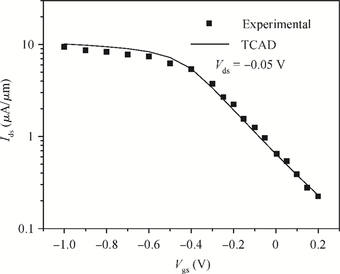
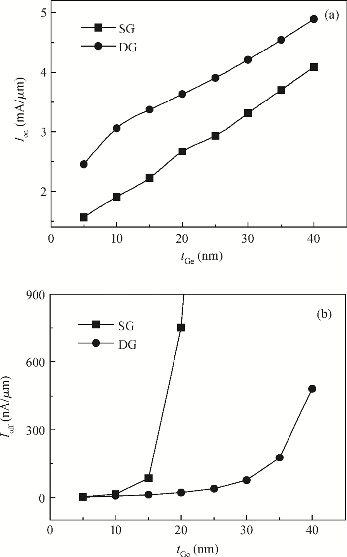
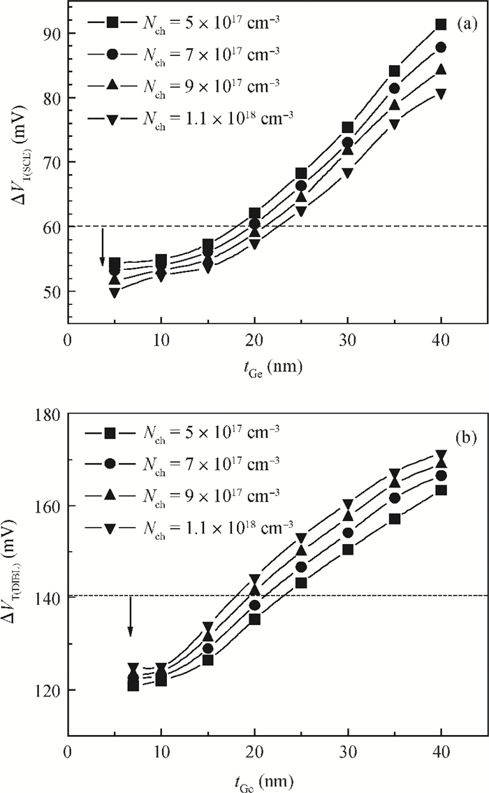
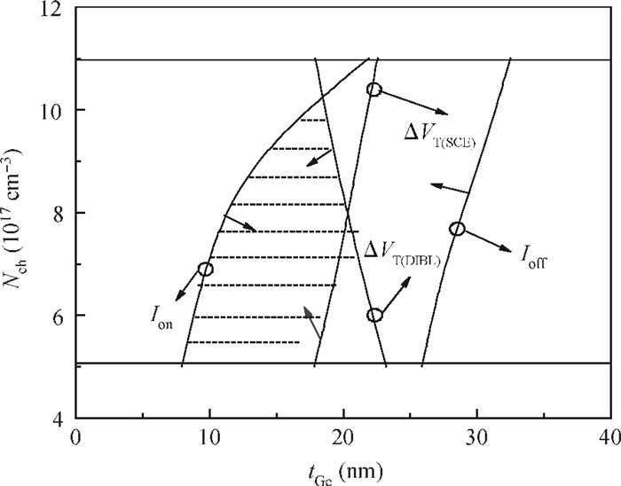
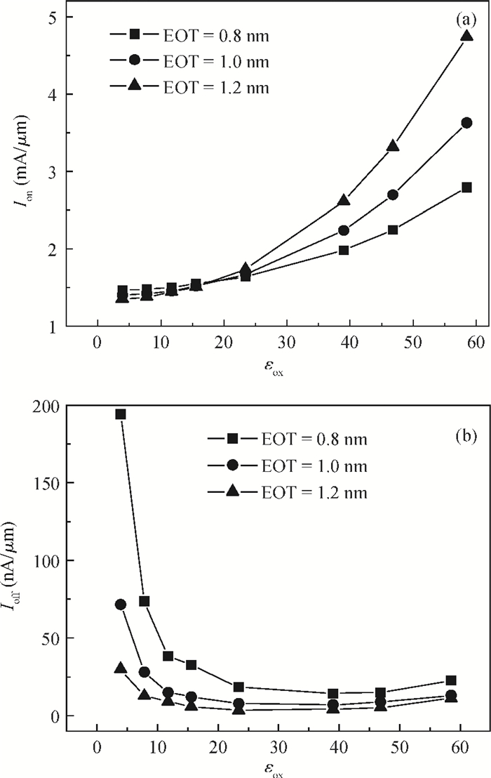
The influences of the main structure and physical parameters of the dual-gate GeOI MOSFET on the device performance are investigated by using a TCAD 2D device simulator. A reasonable value range of germanium (Ge) channel thickness, doping concentration, gate oxide thickness and permittivity is determined by analyzing the on-state current, off-state current, short channel effect (SCE) and drain-induced barrier lowering (DIBL) effect of the GeOI MOSFET. When the channel thickness and its doping concentration are 10-18 nm and (5-9)×1017 cm-3, and the equivalent oxide thickness and permittivity of the gate dielectric are 0.8-1 nm and 15-30, respectively, excellent device performances of the small-scaled GeOI MOSFET can be achieved:on-state current of larger than 1475 μA/μm, off-state current of smaller than 0.1 μA/μm, SCE-induced threshold-voltage drift of lower than 60 mV and DIBL-induced threshold-voltage drift of lower than 140 mV.


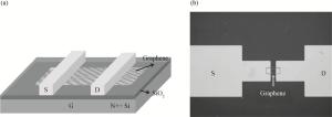
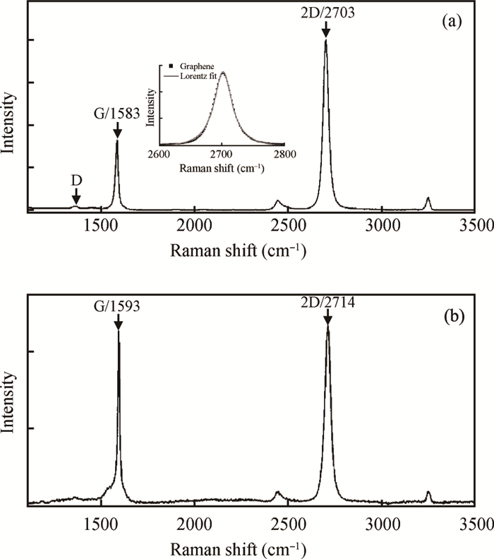
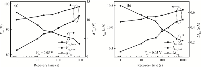
The current transport characteristic is studied systematically based on a back-gate graphene field effect transistor, under repeated test and gate voltage stress. The interface trapped charges caused by the gate voltage sweep process screens the gate electric field, and results in the neutral point voltage shift between the forth and back sweep direction. In the repeated test process, the neutral point voltage keeps increasing with test times in both forth and back sweeps, which indicates the existence of interface trapped electrons residual and accumulation. In gate voltage stress experiment, the relative neutral point voltage significantly decreases with the reducing of stress voltage, especially in -40 V, which illustrates the driven-out phenomenon of trapped electrons under negative voltage stress.


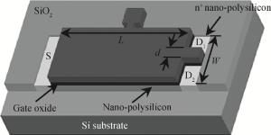
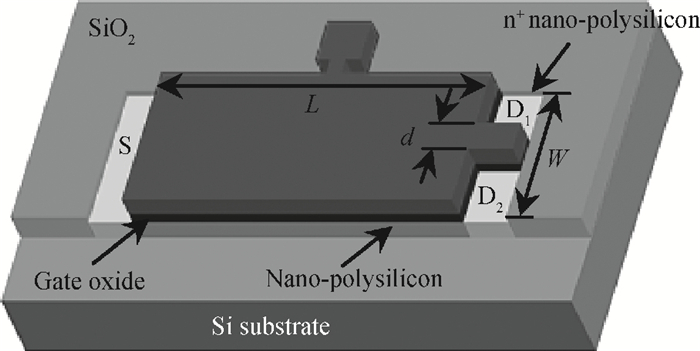
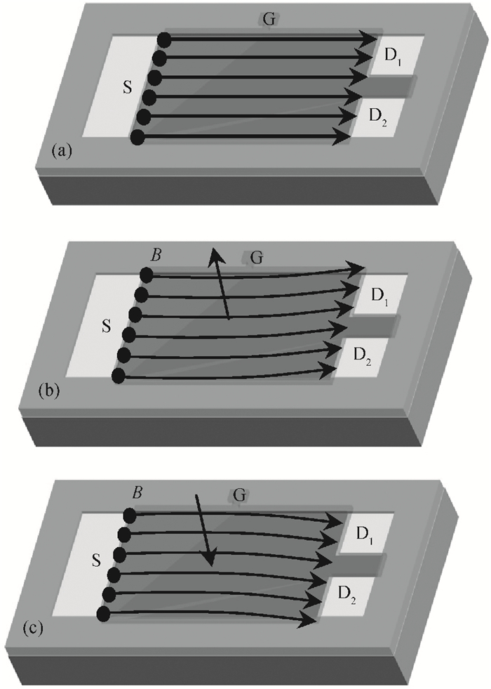
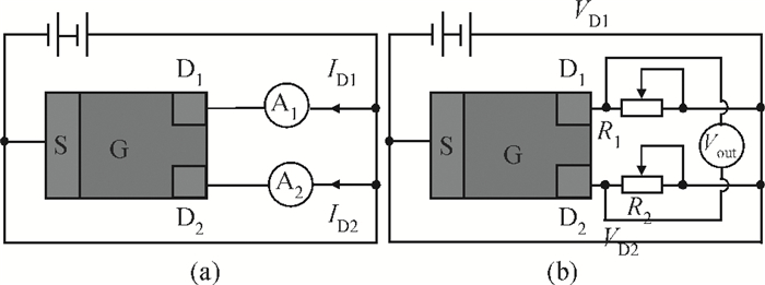
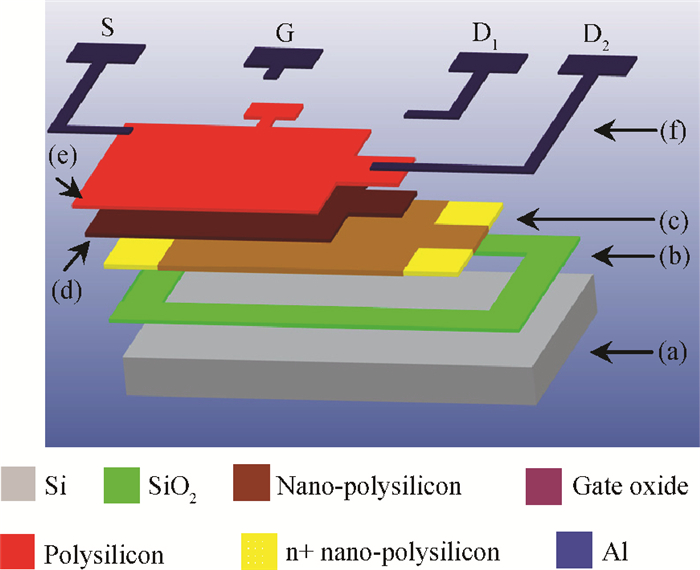
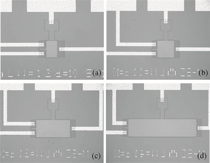
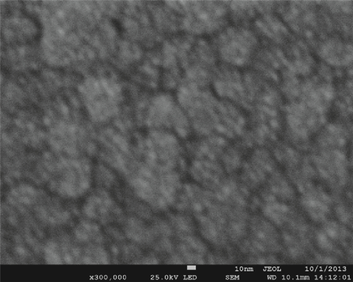
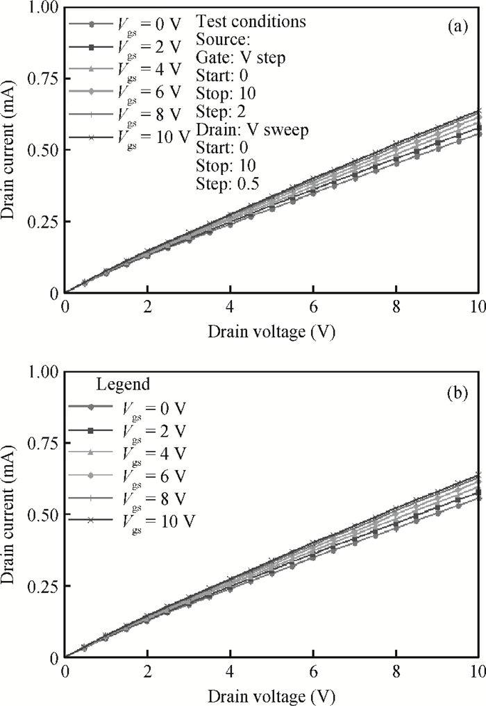
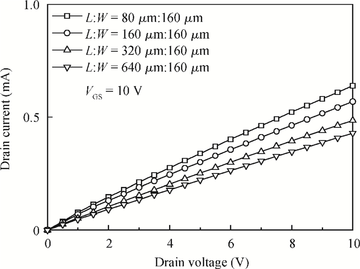
A split-drain magnetic field-effect transistor (MAGFET) based on a nano-polysilicon thin film transistor (TFT) is proposed, which contains one source, two drains and one gate. The sensor chips were fabricated on < 100angle high resistivity silicon substrate by CMOS technology. When drain-source voltage equals 5.0 V and length and width ratio of the TFT channel is 80 μm/160 μm, the current and voltage magnetic sensitivities of the split-drain MAGFET based on the TFT are 0.018 mA/T and 55 mV/T, respectively. Through adopting nano-polysilicon thin films and nano-polysilicon thin films/high resistivity silicon heterojunction interfaces as the magnetic sensing layers, it is possible to realize detection of the external magnetic field. The test results show that magnetic sensitivity of the split-drain MAGFET can be improved significantly.


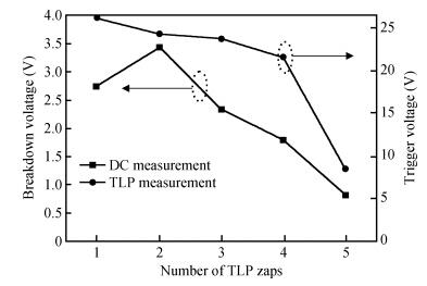
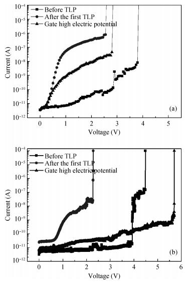
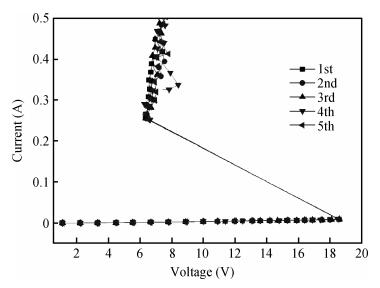
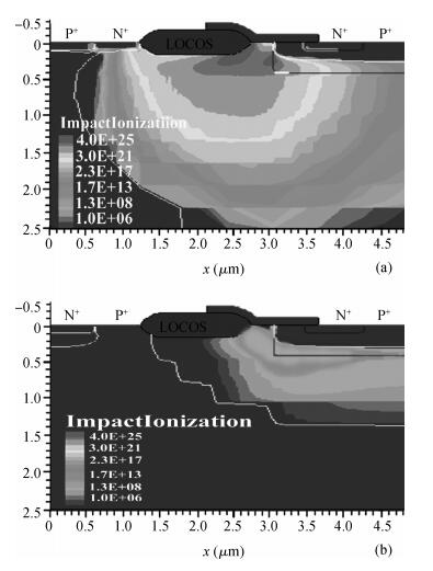
The trigger voltage walk-in effect has been investigated by designing two different laterally diffused metal-oxide-semiconductor (LDMOS) transistors with an embedded silicon controlled rectifier (SCR). By inserting a P+ implant region along the outer and the inner boundary of the N+ region at the drain side of a conventional LDMOS transistor, we fabricate the LDMOS-SCR and the SCR-LDMOS devices with a different triggering order in a 0.5 μm bipolar-CMOS-DMOS process, respectively. First, we perform transmission line pulse (TLP) and DC-voltage degradation tests on the LDMOS-SCR. Results show that the trigger voltage walk-in effect can be attributed to the gate oxide trap generation and charge trapping. Then, we perform TLP tests on the SCR-LDMOS. Results indicate that the trigger voltage walk-in effect is remarkably reduced. In the SCR-LDMOS, the embedded SCR is triggered earlier than the LDMOS, and the ESD current is mainly discharged by the parasitic SCR structure. The electric potential between the drain and the gate decreases significantly after snapback, leading to decreased impact ionization rates and thus reduced trap generation and charge trapping. Finally, the above explanation of the different trigger voltage walk-in behavior in LDMOS-SCR and SCR-LDMOS devices is confirmed by TCAD simulation.


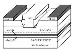
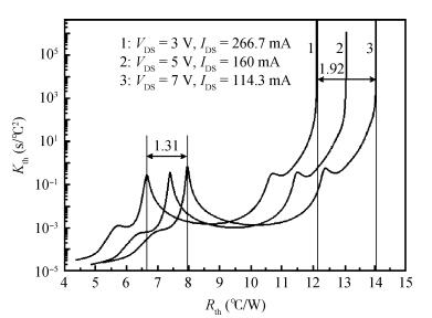
The effect of drain-source voltage on AlGaAs/InGaAs PHEMTs thermal resistance is studied by experimental measuring and simulation. The result shows that AlGaAs/InGaAs PHEMTs thermal resistance presents a downward trend under the same power dissipation when the drain-source voltage (VDS) is decreased. Moreover, the relatively low VDS and large drain-source current (IDS) result in a lower thermal resistance. The chip-level and package-level thermal resistance have been extracted by the structure function method. The simulation result indicated that the high electric field occurs at the gate contact where the temperature rise occurs. A relatively low VDS leads to a relatively low electric field, which leads to the decline of the thermal resistance.


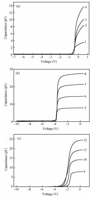
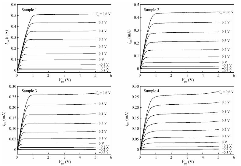
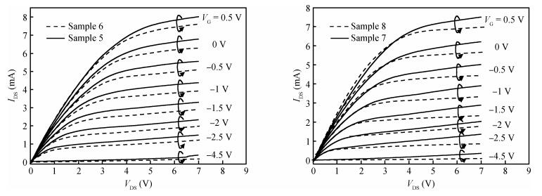
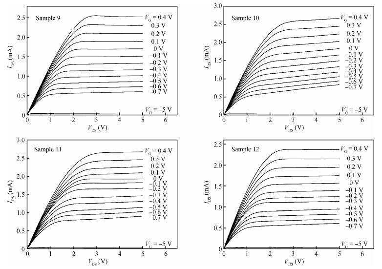
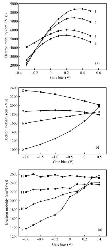
Using the measured capacitance-voltage curves of Ni/Au Schottky contacts with different areas and the current-voltage characteristics for the AlGaAs/GaAs, AlGaN/AlN/GaN and In0.18Al0.82N/AlN/GaN heterostructure field-effect transistors (HFETs) at low drain-source voltage, the two-dimensional electron gas (2DEG) electron mobility for the prepared HFETs was calculated and analyzed. It was found that there is an obvious difference for the variation trend of the mobility curves between the Ⅲ-Ⅴ nitride HFETs and the AlGaAs/GaAs HFETs. In the Ⅲ-Ⅴ nitride HFETs, the variation trend for the curves of the 2DEG electron mobility with the gate bias is closely related to the ratio of the gate length to the drain-to-source distance. While the ratio of the gate length to the drain-to-source distance has no effect on the variation trend for the curves of the 2DEG electron mobility with the gate bias in the AlGaAs/GaAs HFETs. The reason is attributed to the polarization Coulomb field scattering in the Ⅲ-Ⅴ nitride HFETs.


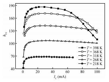
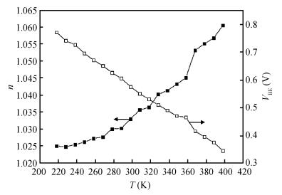
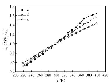
Considering the impacts of ideal factor n, VBE and band gap changes with the temperature on current gain, the current gain expression has been corrected to make the results closer to the actual test. Besides, the accelerating lifetime study method in the constant temperature-humidity stress is used to estimate the reliability of the same batch transistors. Applying the revised findings from the expression, the current gains before and after the test are compared and analyzed, and, according to the degradation data of the current gain, the transistor lifetimes in the test stress are respectively extrapolated in the different failure criteria.


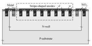
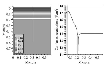
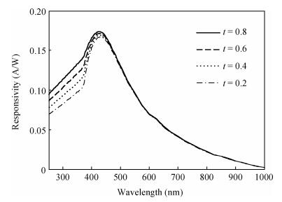
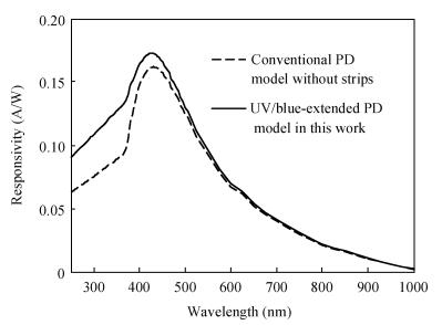
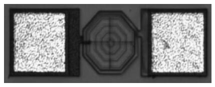
A CMOS UV and blue-extended photodiode is presented and fabricated for light detection in the ultraviolet/blue spectral range. An octagon homocentric ring-shaped geometry is used to improve the ultraviolet responsivity and suppress edge breakdown. This paper has established a two-dimensional responsivity physical model for the presented photodiode and given some numerical analyses. The dead layer effect, which is caused by the high-doping effects and boron redistribution, is considered when analyzing the distribution of the current of the proposed UV and blue-extended photodiode. In the dead layer, the boron doping profile decreases towards the surface. Simulated results illustrate that the responsivity in the UV range is obviously decreased by the effect of the dead layer, while it is not affected in the visible and near-infrared part of the spectrum. The presented photodiode is fabricated and the silicon tested results are given, which agree well with the simulated ones.


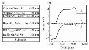
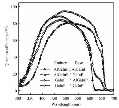
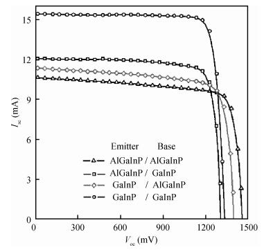
An Al0.13GaInP sub-cell used as the top cell in the next generation of high efficiency multi-junction solar cells is fabricated. An efficiency of 10.04% with 1457.3 mV in Voc and 11.9 mA/cm2 in Isc was obtained. QE comparison was carried out to verify the influence of an O-related defect introduced by the high Al-content materials on the cell performance during MOCVD growth. Hetero-structures are employed to confirm the origin of the decreasing short circuit current density compared to a GaInP single junction solar cell. An effective method to improve the performance of broadband solar cells by increasing Isc with a cost of Voc was proposed.


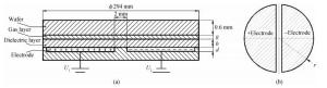
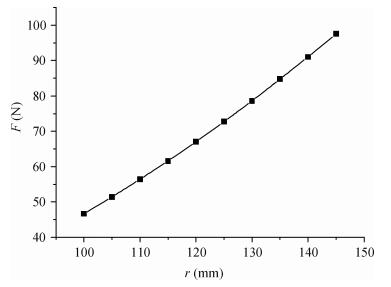
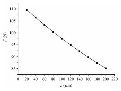
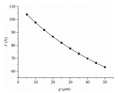
As one of the core components of IC manufacturing equipment, the electrostatic chuck (ESC) has been widely applied in semiconductor processing such as etching, PVD and CVD. The clamping force of the ESC is one of the most important technical indicators. A multi-physics simulation software COMSOL is used to analyze the factors influencing the clamping force. The curves between the clamping force and the main parameters such as DC voltage, electrode thickness, electrode radius, dielectric thickness and helium gap are obtained. Moreover, the effects of these factors on the clamping force are investigated by means of orthogonal experiments. The results show that the factors can be ranked in order of voltage, electrode radius, helium gap and dielectric thickness according to their importance, which may offer certain reference for the design of ESCs.


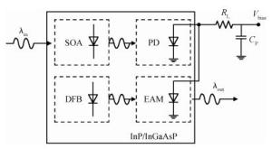
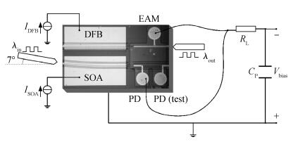
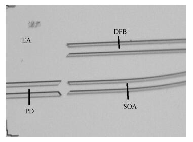
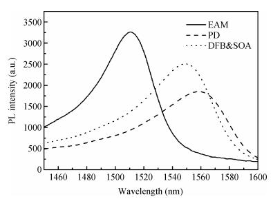
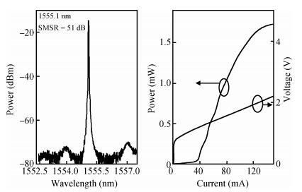
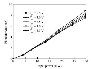
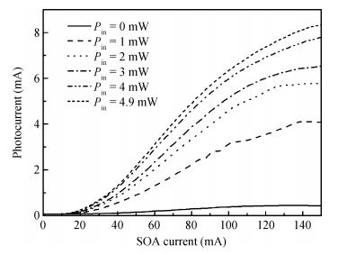
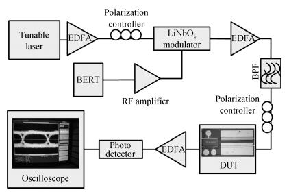
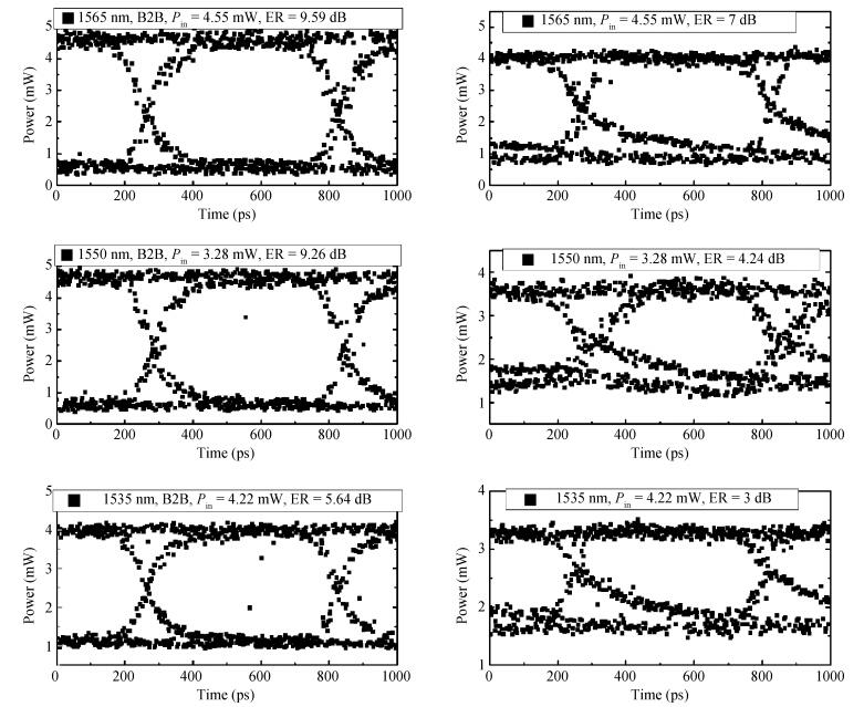
A selected area growth wavelength converter based on a PD-EAM optical logic gate for WDM application is presented, integrating an EML transmitter and a SOA-PD receiver. The design, fabrication, and DC characters were analyzed. A 2 Gb/s NRZ signal based on the C-band wavelength converted to 1555 nm with the highest extinction ratio of 7 dB was achieved and wavelength converted eye diagrams with eyes opened were presented.


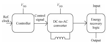
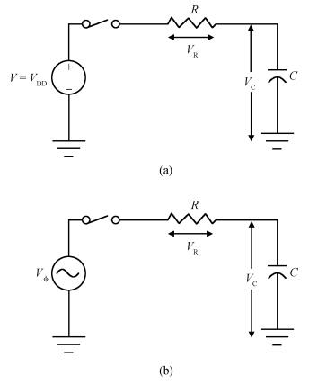
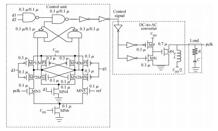
We analyze the energy performance of a complete adiabatic circuit/system including the Power Clock Generator (PCG) at the 90 nm CMOS technology node. The energy performance in terms of the conversion efficiency of the PCG is extensively carried out under the variations of supply voltage, process corner and the driver transistor's width. We propose an energy-efficient singe cycle control circuit based on the two-stage comparator for the synchronous charge recovery sinusoidal power clock generator (PCG). The proposed PCG is used to drive the 4-bit adiabatic Ripple Carry Adder (RCA) and their simulation results are compared with the adiabatic RCA driven by the reported PCG. We have also simulated the logically equivalent static CMOS RCA circuit to compare the energy saving of adiabatic and non-adiabatic logic circuits. In the clock frequency range from 25 MHz to 1GHz, the proposed PCG gives a maximum conversion efficiency of 56.48%. This research work shows how the design of an efficient PCG increases the energy saving of adiabatic logic.


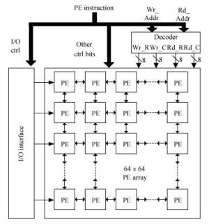
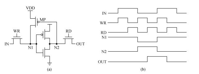
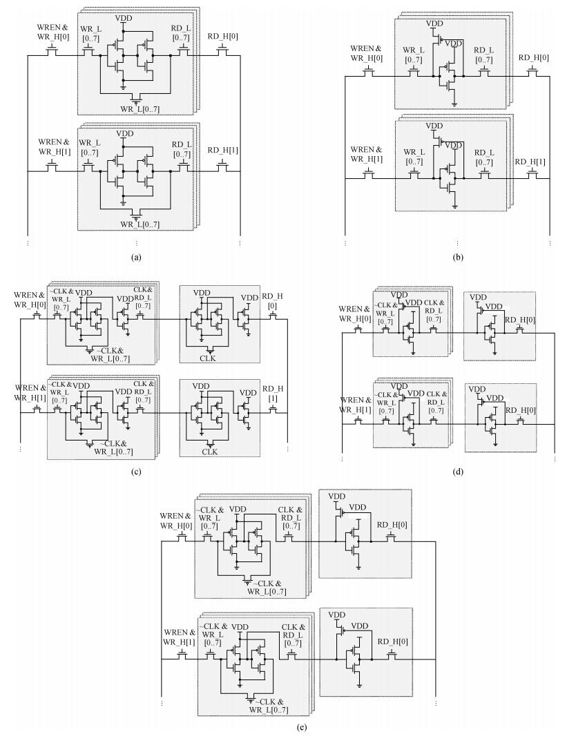
This paper presents a novel compact memory in the processing element (PE) for single-instruction multiple-data (SIMD) vision chips. The PE memory is constructed with 8×8 register cells, where one latch in the slave stage is shared by eight latches in the master stage. The memory supports simultaneous read and write on the same address in one clock cycle. Its compact area of 14.33 μm2/bit promises a higher integration level of the processor. A prototype chip with a 64×64 PE array is fabricated in a UMC 0.18 μm CMOS technology. Five types of the PE memory cell structure are designed and compared. The testing results demonstrate that the proposed PE memory architecture well satisfies the requirement of the vision chip in high-speed real-time vision applications, such as 1000 fps edge extraction.


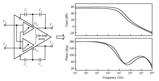
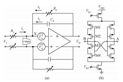
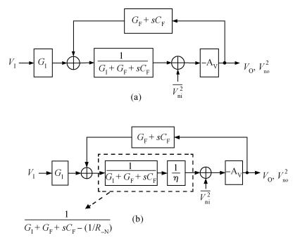
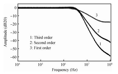
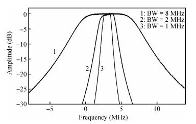
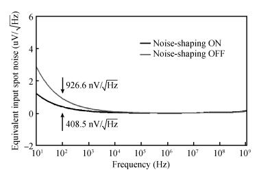
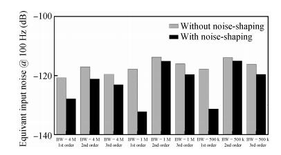
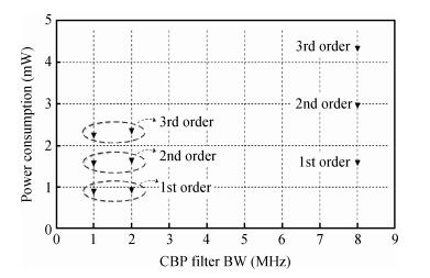
A reconfigurable complex band-pass (CBP)/low-pass (LP) active-RC filter with a noise-shaping technique for wireless receivers is presented. Its bandwidth is reconfigurable among 500 kHz, 1 MHz and 4 MHz in LP mode and 1 MHz, 2 MHz and 8 MHz in CBP mode with 3 MHz center frequency. The Op-Amps used in the filter are realized in cell arrays in order to obtain scalable power consumption among the different operation modes. Furthermore, the filter can be configured into the 1st order, 2nd order or 3rd order mode, thus achieving a flexible filtering property. The noise-shaping technique is introduced to suppress the flicker noise contribution. The filter has been implemented in 180 nm CMOS and consumes less than 3 mA in the 3rd 8 MHz-bandwidth CBP mode. The spot noise at 100 Hz can be reduced by 14.4 dB at most with the introduced noise-shaping technique.


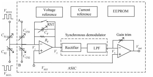
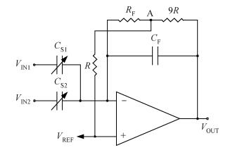
A high stability in-circuit reprogrammable technique control system for a capacitive MEMS accelerometer is presented. Modulation and demodulation are used to separate the signal from the low frequency noise. A low-noise low-offset charge integrator is employed in this circuit to implement a capacitance-to-voltage converter and minimize the noise and offset. The application-specific integrated circuit (ASIC) is fabricated in a 0.5 μm one-ploy three-metal CMOS process. The measured results of the proposed circuit show that the noise floor of the ASIC is -116 dBV, the sensitivity of the accelerometer is 66 mV/g with a nonlinearity of 0.5%. The chip occupies 3.5×2.5 mm2 and the current is 3.5 mA.


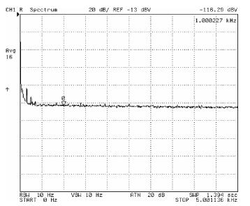
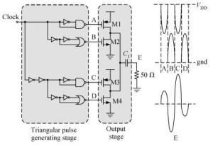
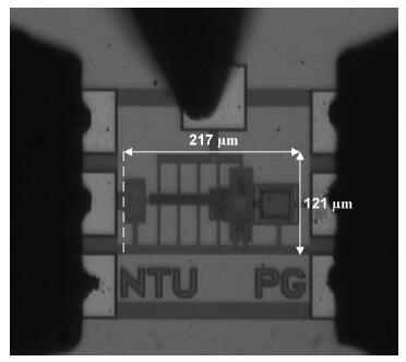
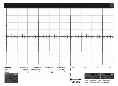
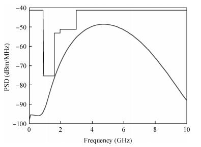
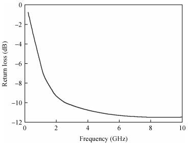
A CMOS fifth-derivative Gaussian pulse generator is presented for ultra-wideband (UWB) applications. The design exhibits low power consumption, low circuit complexity, and a precise pulse shape to inherently comply with the FCC spectrum mask for indoor UWB applications without the need for a filter. The pulse generator is implemented with a 1.8-V, 0.18-μm CMOS process. The small core chip size of the pulse generator is only 217×121 μm2 because of its all digital circuit design. The measured fifth-derivative Gaussian pulse has a peak-to-peak amplitude of 158 mV and a pulse width of 800 ps. The average power dissipation is 0.6 mW with a pulse repetition frequency of 50 MHz.


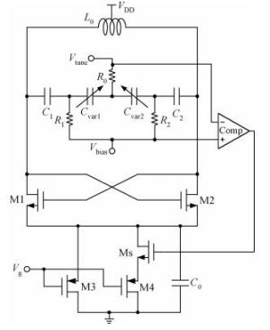
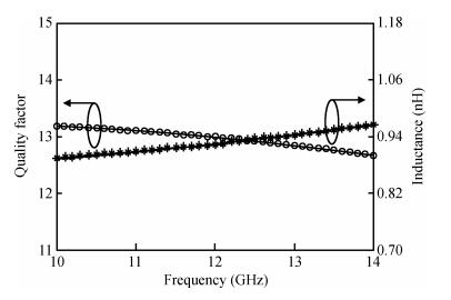
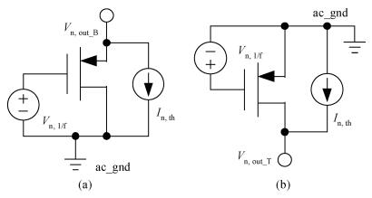
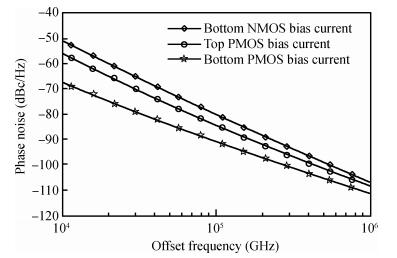
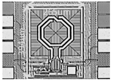
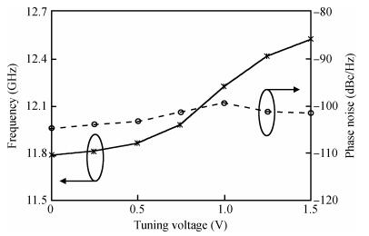
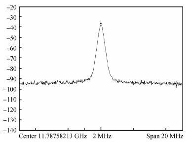
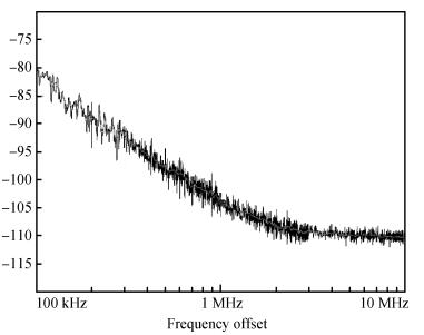
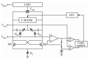
This paper presents the design and implementation of a current self-adjusted VCO with low power consumption. In the proposed VCO, a bottom PMOS current source instead of a top one is adopted to decrease the tail noise. A current self-adjusted technique without additional external control signals is taken to ensure the VCO starts up in the whole band while keeping the power consumption relatively low. Meanwhile, the phase noise of the VCO at the low frequency (high Cvar) can be reduced by the technique. The circuit is implemented in 0.18 μm CMOS technology. The proposed VCO exhibits low power consumption of < 1.6 mW at a 1.5 V supply voltage and a tuning range from 11.79 to 12.53 GHz. The measured phase noise at 1 MHz offset from the frequency 11.79 GHz is -104.7 dBc/Hz, and the corresponding FOM is -184.2 dBc/Hz.


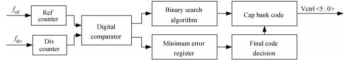
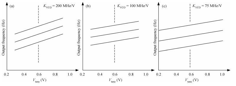
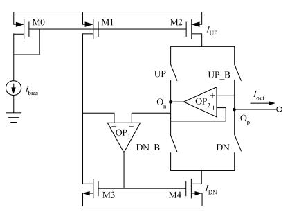
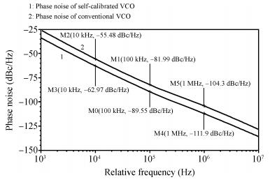
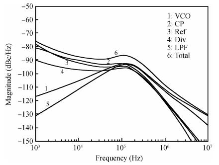
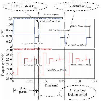
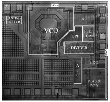
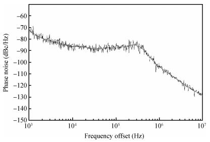
A low noise phase locked loop (PLL) frequency synthesizer implemented in 65 nm CMOS technology is introduced. A VCO noise reduction method suited for short channel design is proposed to minimize PLL output phase noise. A self-calibrated voltage controlled oscillator is proposed in cooperation with the automatic frequency calibration circuit, whose accurate binary search algorithm helps reduce the VCO tuning curve coverage, which reduces the VCO noise contribution at PLL output phase noise. A low noise, charge pump is also introduced to extend the tuning voltage range of the proposed VCO, which further reduces its phase noise contribution. The frequency synthesizer generates 9.75-11.5 GHz high frequency wide band local oscillator (LO) carriers. Tested 11.5 GHz LO bears a phase noise of -104 dBc/Hz at 1 MHz frequency offset. The total power dissipation of the proposed frequency synthesizer is 48 mW. The area of the proposed frequency synthesizer is 0.3 mm2, including bias circuits and buffers.


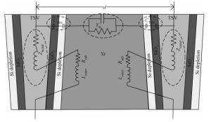
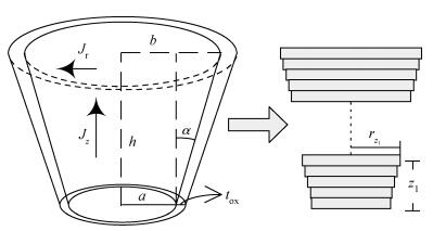
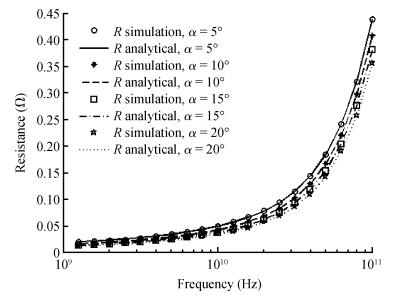
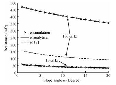
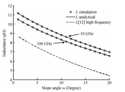
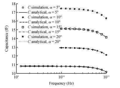
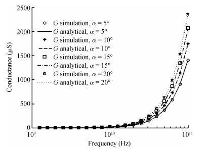
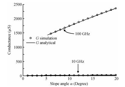
A fast RLGC circuit model with analytical expression is proposed for the dual tapered through-silicon via (TSV) structure in three-dimensional integrated circuits under different slope angles at the wide frequency region. By describing the electrical characteristics of the dual tapered TSV structure, the RLGC parameters are extracted based on the numerical integration method. The RLGC model includes metal resistance, metal inductance, substrate resistance, outer inductance with skin effect and eddy effect taken into account. The proposed analytical model is verified to be nearly as accurate as the Q3D extractor but more efficient.


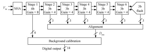
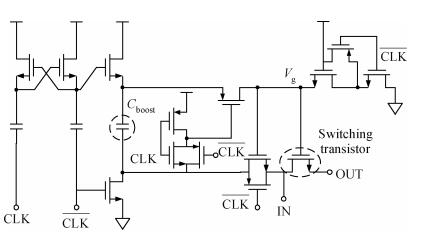
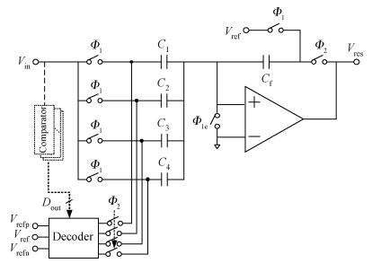
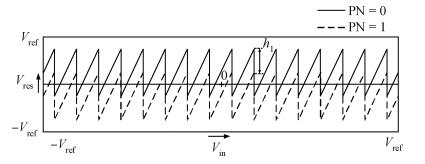
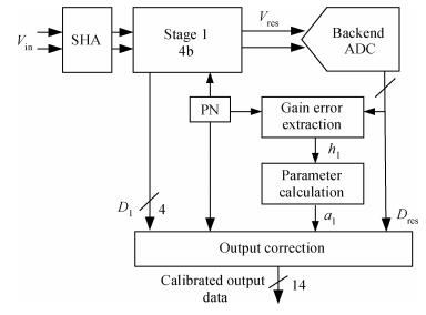
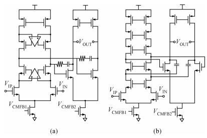
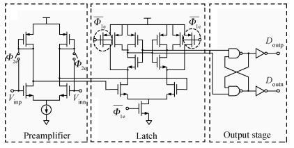
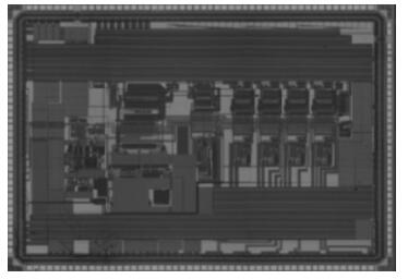
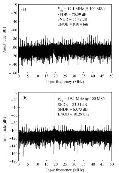
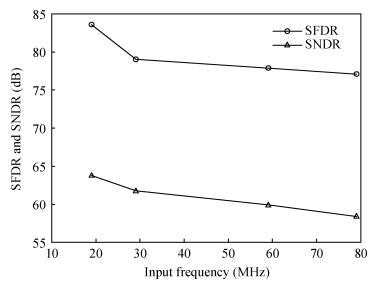
This paper demonstrates a 14-bit 100 MS/s CMOS pipelined analog-to-digital converter (ADC). The nonlinearity model for bootstrapped switches is established to optimize the design parameters of bootstrapped switches, and the calculations based on this model agree well with the measurement results. In order to achieve high linearity, a gradient-mismatch cancelling technique is proposed, which eliminates the first order gradient error of sampling capacitors by combining arrangement of reference control signals and capacitor layout. Fabricated in a 0.18-μm CMOS technology, this ADC occupies 10.16-mm2 area. With statistics-based background calibration of finite opamp gain in the first stage, the ADC achieves 83.5-dB spurious free dynamic range and 63.7-dB signal-to-noise-and distortion ratio respectively, and consumes 393 mW power with a supply voltage of 2 V.


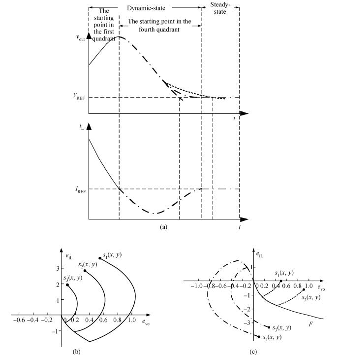
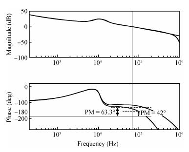
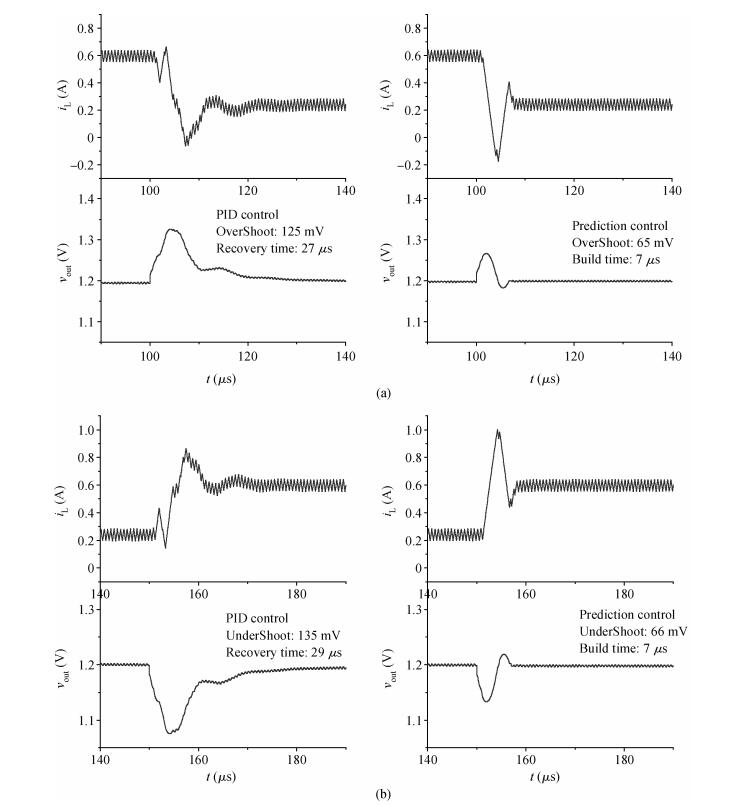
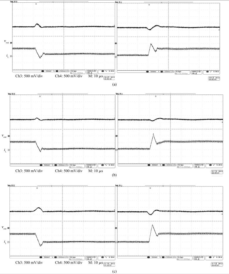
The purpose of this paper is to present a novel trajectory prediction method for proximate time-optimal digital control DC-DC converters. The control method provides pre-estimations of the duty ratio in the next several switching cycles, so as to compensate the computational time delay of the control loop and increase the control loop bandwidth, thereby improving the response speed. The experiment results show that the fastest transient response time of the digital DC-DC with the proposed prediction is about 8 μs when the load current changes from 0.6 to 0.1 A.


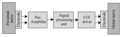
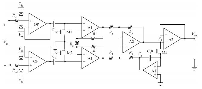
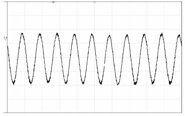
Nerve tracts interruption is one of the major reasons for dysfunction after spiral cord injury. The microelectronic neural bridge is a method to restore function of interrupted neural pathways, by making use of microelectronic chips to bypass the injured nerve tracts. A low-power fully integrated microelectronic neural bridge chip is designed, using CSMC 0.5-μm CMOS technology. The structure and the key points in the circuit design will be introduced in detail. In order to meet the requirement for implantation, the circuit was modified to avoid the use of off-chip components, and fully monolithic integration is achieved. The operating voltage of the circuit is ±2.5 V, and the chip area is 1.21×1.18 mm2. According to the characteristic of neural signal, the time-domain method is used in testing. The pass bandwidth of the microelectronic neural bridge system covers the whole frequency range of the neural signal, power consumption is 4.33 mW, and the gain is adjustable. The design goals are achieved.


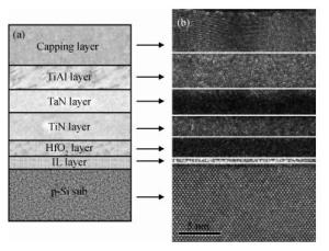
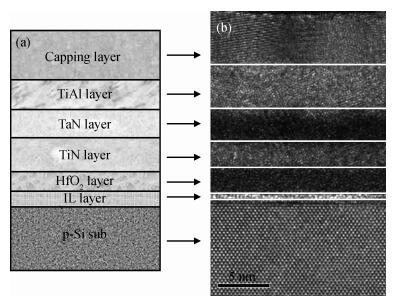
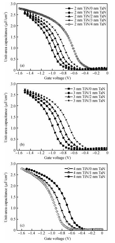
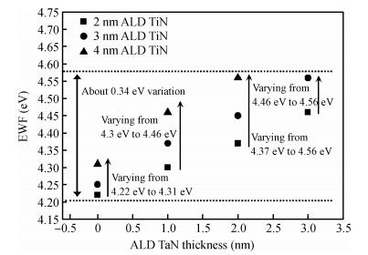
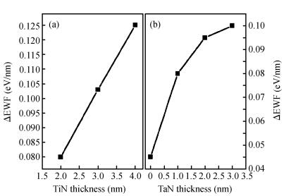
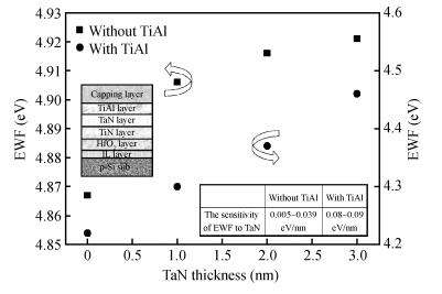
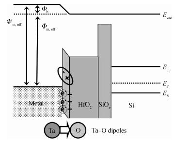
We evaluated the TiN/TaN/TiAl triple-layer to modulate the effective work function (EWF) of a metal gate stack for the n-type metal-oxide-semiconductor (NMOS) devices application by varying the TiN/TaN thickness. In this paper, the effective work function of EWF ranges from 4.22 to 4.56 eV with different thicknesses of TiN and TaN. The thinner TiN and/or thinner in situ TaN capping, the closer to conduction band of silicon the EWF is, which is appropriate for 2-D planar NMOS. Mid-gap work function behavior is observed with thicker TiN, thicker in situ TaN capping, indicating a strong potential candidate of metal gate material for replacement gate processed three-dimensional devices such as FIN shaped field effect transistors. The physical understandings of the sensitivity of EWF to TiN and TaN thickness are proposed. The thicker TiN prevents the Al diffusion then induces the EWF to shift to mid-gap. However, the TaN plays a different role in effective work function tuning from TiN, due to the Ta-O dipoles formed at the interface between the metal gate and the high-k layer.
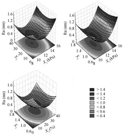
Firstly, this paper presents an orthogonal test of six factors and five levels, called the chemical mechanical polishing (CMP) process parameters experiment, for determining the best process parameters and ranking the influencing factors from primary to secondary. The three most important factors are the polishing pressure, the polishing liquid concentration and the relative velocity ratio of polishing disk to polishing carrier. Then, based on this analysis, the three factors and three levels of the quadratic orthogonal regression test are put forward. A mathematical model impacting the surface roughness has also been set up. Finally, this work has achieved a polished wafer, whose material removal rate (MRR) is in the range of 70-90 nm/h and the surface roughness (Ra) is between 0.3 nm and 0.5 nm.


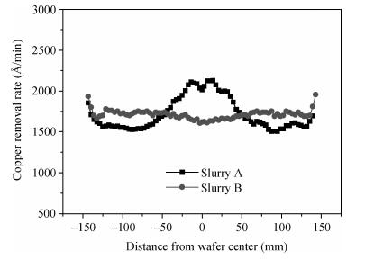
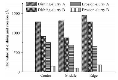
The copper removal rate and uniformity of two types copper slurries were investigated, which was performed on the 300 mm chemical mechanical planarization (CMP) platform. The experiment results illustrate that the removal rate of the two slurries is nearly the same. Slurry A is mainly composed of a FA/OⅡ type chelating agent and the uniformity reaches to 88.32%. While the uniformity of slurry B is 96.68%, which is mainly composed of a FA/OV type chelating agent. This phenomenon demonstrates that under the same process conditions, the uniformity of different slurries is vastly different. The CMP performance was evaluated in terms of the dishing and erosion values. In this paper, the relationship between the uniformity and the planarization was deeply analyzed, which is mainly based on the endpoint detection mechanism. The experiment results reveal that the slurry with good uniformity has low dishing and erosion. The slurry with bad uniformity, by contract, increases Cu dishing significantly and causes copper loss in the recessed region. Therefore, the following conclusions are drawn:slurry B can improve the wafer leveling efficiently and minimize the resistance and current density along the line, which is helpful to improve the device yield and product reliability. This investigation provides a guide to improve the uniformity and achieve the global and local planarization. It is very significant to meet the requirements for 22 nm technology nodes and control the dishing and erosion efficiently.