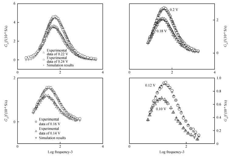
The admittance measurements of a hetero-junction can be used to derive the density of the interfacial state in the hetero-junction. Hence, prediction conductance via frequency is very useful for comprehension of the admittance of a hetero-junction using a mathematical strategy. From the observations on the curve of the frequency-dependent conductance of the hetero-junction an analytic model with four-parameters was developed that relates conductance to frequency; the theoretical results agree quite well with the experimental data. The model shows potential for a variety of applications including different electronic devices. The model is a practical tool that can be readily used for assessing the electronic behaviors of a hetero-junction and is scientifically justifiable. In addition, the mathematical bridge to link the density of the interfacial state of the (pyronine-B)/p-Si structure to energy implies a good route to discuses the density of the interfacial state of interfaces.


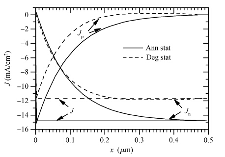
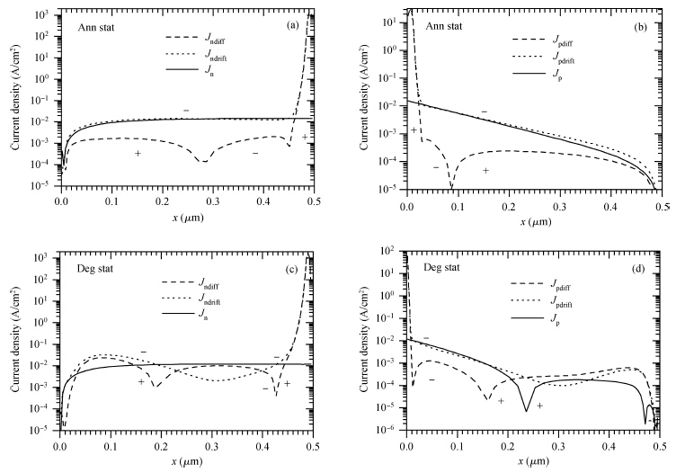
In this work, a comprehensive model that takes the phenomenon of carrier thermionic-emission within the frame work of a diffusion theory of current conducting into account in the type II hetero-junction CdTe solar cell is developed. According to this model, it is found that the total current flowing through the CdTe solar cell is limited by the thermionic process for very thin quasi-neutral regions and limited by the diffusion process for the reverse case. In future research of the CdTe solar cell, such an approach may enable the determination of the boundary conditions for all doping profiles and computation of the conversion efficiency, etc.

The structural properties, band structures and densities of states of Sn-doped Ga1.375In0.625O3 with a Sn atom substituting for the Ga atom or a Sn atom substituting for the In atom are calculated by using the first-principles method. The substitution of the Sn atom for the Ga atom in Ga1.375In0.625O3 (Ga1.25In0.625Sn0.125O3) has larger lattice parameters and stronger Sn-O ionic bonds than that of the substitutional doping of the Sn atom for the In atom in Ga1.375In0.625O3 (Ga1.375In0.5Sn0.125O3). Results show that the Sn atom is preferentially substituted for the In atom in Sn-doped Ga1.375In0.625O3. Sn-doped Ga1.375In0.625O3 exhibits n-type metallic conductivity, and the impurity bands are mainly provided by the Sn 5s states. The optical band gap of Ga1.375In0.5Sn0.125O3 is larger than that of Ga1.25In0.625Sn0.125O3. Ga1.25In0.625Sn0.125O3 has a smaller electron effective mass and a slightly larger mobility. However, Ga1.375In0.5Sn0.125O3 has a larger relative electron number and a slightly higher conductivity.

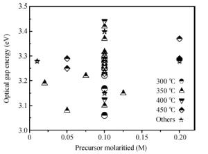
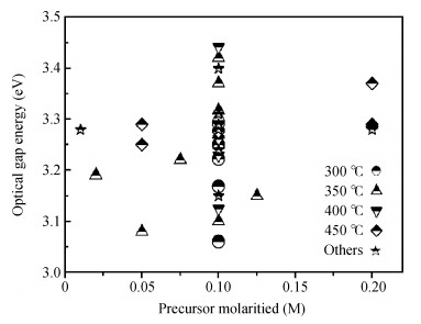
We investigated the optical properties of undoped zinc oxide thin films as the n-type semiconductor; the thin films were deposited at different precursor molarities by ultrasonic spray and spray pyrolysis techniques. The thin films were deposited at different substrate temperatures ranging between 200 and 500 ℃. In this paper, we present a new approach to control the optical gap energy of ZnO thin films by concentration of the ZnO solution and substrate temperatures from experimental data, which were published in international journals. The model proposed to calculate the band gap energy with the Urbach energy was investigated. The relation between the experimental data and theoretical calculation suggests that the band gap energies are predominantly estimated by the Urbach energies, film transparency, and concentration of the ZnO solution and substrate temperatures. The measurements by these proposal models are in qualitative agreements with the experimental data; the correlation coefficient values were varied in the range 0.96–0.99999, indicating high quality representation of data based on Equation (2), so that the relative errors of all calculation are smaller than 4%. Thus, one can suppose that the undoped ZnO thin films are chemically purer and have many fewer defects and less disorder owing to an almost complete chemical decomposition and contained higher optical band gap energy.


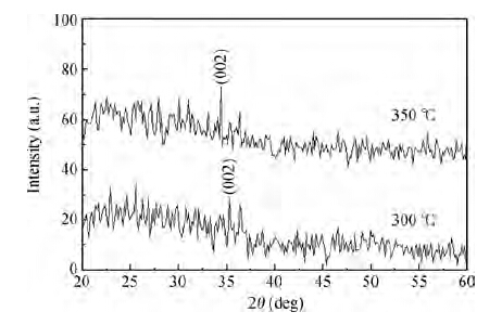
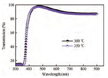
Zinc oxide (ZnO) thin films were deposited on glass substrates by spray pyrolysis technique decomposition of zinc acetate dihydrate in an ethanol solution with 30 mL of deposition rate, the ZnO thin films were deposited at two different temperatures: 300 and 350 ℃. The substrates were heated using the solar cells method. The substrate was R217102 glass, whose size was 30 × 17.5 × 1 mm3. The films exhibit a hexagonal wurtzite structure with a strong (002) preferred orientation. The higher value of crystallite size is attained for sprayed films at 350 ℃, which is probably due to an improvement of the crystallinity of the films at this point. The average trans mittance of obtain films is about 90%-95%, as measured by a UV-vis analyzer. The band gap energy varies from 3.265 to 3.294 eV for the deposited ZnO thin film at 300 and 350 ℃, respectively. The electrical resistivity measured of our films are in the order 0.36 Ω·cm.


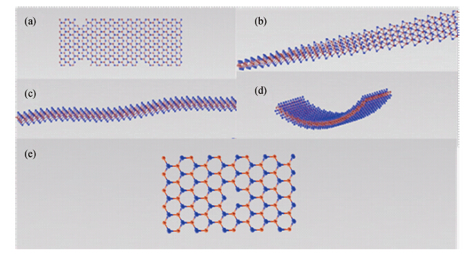
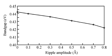
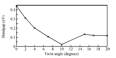
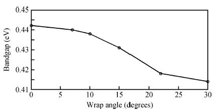
We have studied the WS2 armchair nanoribbon with various defects like vacancy, edge roughness, twist, turn and ripple and compared how the bandgap changes due to such defects with the bandgap of a nanoribbon with no defects. Materials like WS2 and other transition metal dichalcogenides (MX2) have a graphene like layered structure with hexagonal rings and have properties that have attracted a lot of interest. Hence it is essential to study the changes in the band structure of the nanoribbon of WS2 due to the inclusion of defects like vacancy, rough edge, wrap, ripple and twist for making any device based on WS2.


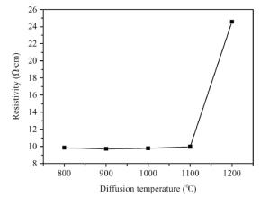
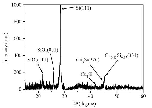
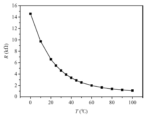
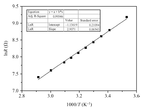
Copper doped n-type single-crystal silicon materials are prepared by a high temperature diffusion process. The electrical and thermal-sensitive characteristic of materials is investigated under different experimental conditions. The results show that the maximum resistivity of 46.2 Ω ·cm is obtained when the sample is treated at 1200 ℃ for 2 h with the surface concentration of the copper dopant source being 1.83 × 10⁻⁷ mol/cm2. The copper doped n-type silicon material presents a negative temperature-sensitive characteristic and the B values are about 3010-4130 K.


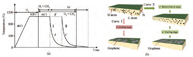
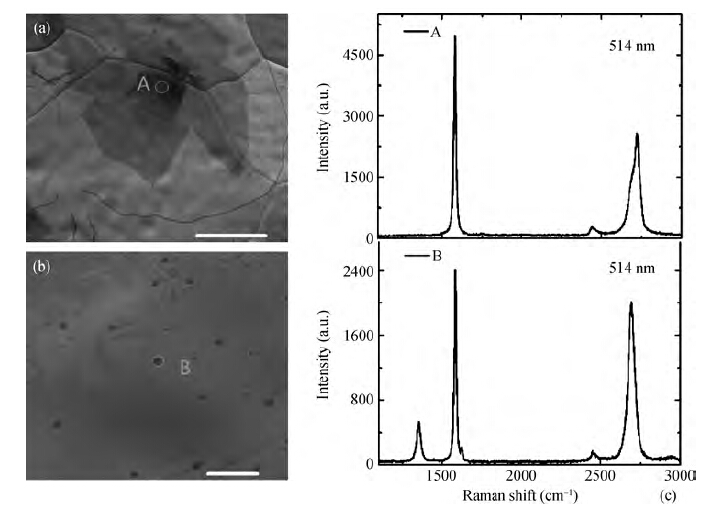
The two-dimensional material graphene shows its extraordinary potential in many application fields. As the most effective method to synthesize large-area monolayer graphene, chemical vapor deposition has been well developed; however, it still faces the challenge of a high occurrence of multilayer graphene, which causes the small effective area of monolayer graphene. This phenomenon limits its applications in which only a big size of monolayer graphene is needed. In this paper, by introducing a redistribution stage after the decomposition of carbon source gas to redistribute the carbon atoms dissolved in Pt foils, the number of multilayer flakes on the monolayer graphene decreases. The mean area of monolayer graphene can be extended to about 16 000 μm2, which is eight times larger than that of the graphene grown without the redistribution stage. A Raman spectrograph is used to demonstrate the high quality of the monolayer graphene grown by the improved process.


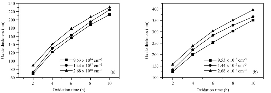
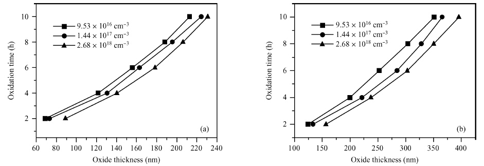
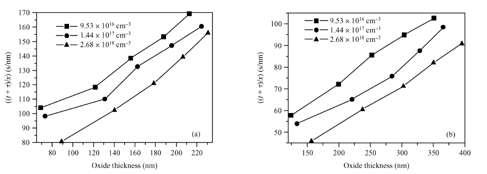
The doping dependence of dry thermal oxidation rates in n-type 6H-SiC was studied. The oxidation temperature ranged from 1050 to 1150 ℃ and the nitrogen doping concentration ranged from 9.53 × 10¹⁶, 1.44 × 10¹⁷, to 2.68 × 1018 cm-3. By combining the modified deal-grove model and Arrhenius equation, the linear and parabolic rate constants, and their corresponding activation energies were extracted. The results show that: higher temperature corresponded to thicker oxides; dry thermal oxidation rate in n-type 6H-SiC depended on the doping concentration; both linear-rate-constant and parabolic-rate-constant increased with the doping concentration; the parabolic activation energy increased from 0.082 to 0.104 eV, both linear and parabolic activation energies increasing with the doping concentration; and, the parabolic pre-exponential factor increased from 2.6 × 10⁴ to 2.7 × 10⁵ nm2/s, both linear and parabolic pre-exponential factor increasing with doping concentration. Moreover, the experiment also illustrated that it is unreasonable to use a variation of the Arrhenius activation energy to explain the doping dependence of thermal oxidation on SiC.

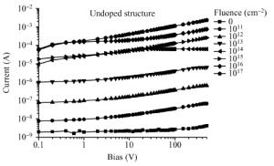
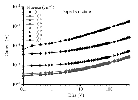
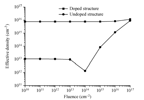
We have carried out a numerical simulation of the effect of gold doping on the electrical characteristics of long silicon diodes exposed to neutron irradiation. The aim is to investigate the effect of gold on the hardness of the irradiated diodes. The reverse current voltage and capacitance voltage characteristics of doped and undoped diodes are calculated for different irradiation doses. The leakage current and the effective doping density are extracted from these two characteristics respectively. The hardness of the diodes is evaluated from the evolution of the leakage current and the effective doping density with irradiation doses. It was found that diodes doped with gold are less sensitive to irradiation than undoped ones. Thus gold appears to stabilise the electrical properties on irradiation. The conduction mechanism is studied by the evolution of the current with temperature. The evaluated activation energy indicates that as the gold doping or irradiation dose increases, the current switches from the basic diffusion to the generation-recombination process, and that it can even become ohmic for very high gold densities or irradiation doses.


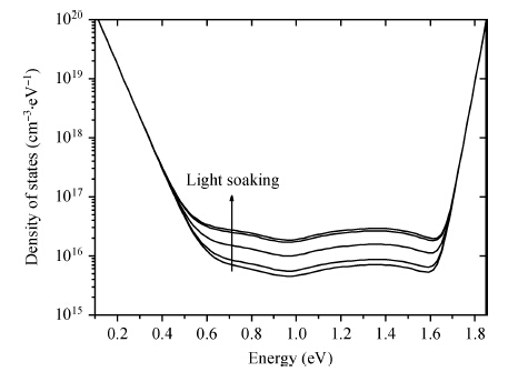
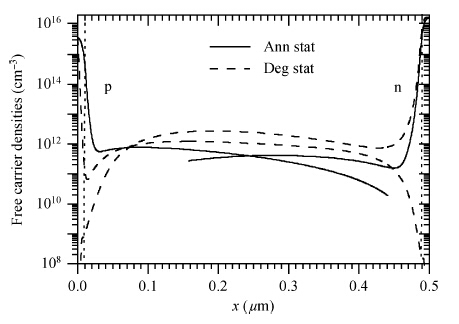
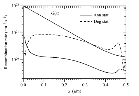
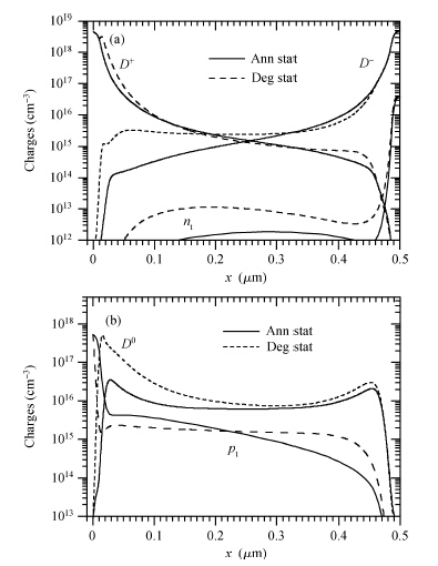
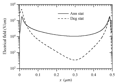
Using a previous model, which was developed to describe the light-induced creation of the defect density in the a-Si:H gap states, we present in this work a numerical modelling of the photodegradation effect in the a-Si:H p-i-n solar cell under continuous illumination. We first considered the simple case of a monochromatic light beam with a wavelength λ between 530-540 nm non uniformly absorbed, then the global standard solar spectrum (AM 1.5) illumination is taken into account. The photodegradation is analysed on the basis of the resulting changes in the free carrier's densities, recombination rate, band structure, electrical potential and field, space charge, and current densities. Changes in the cell's external parameters: the open circuit voltage Voc, the short circuit current density Jsc, the fill factor FF and the maximum power density Pmax are also presented.


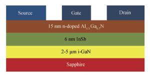
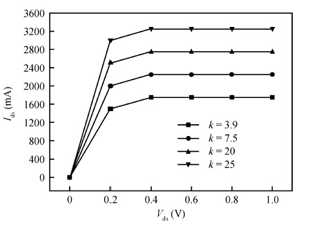
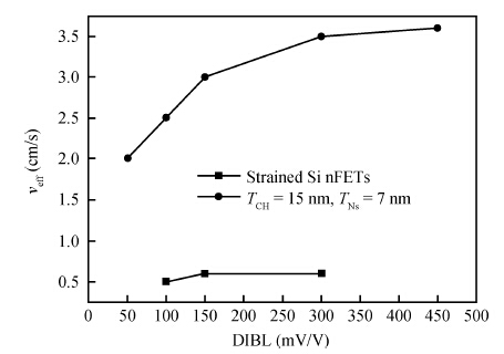
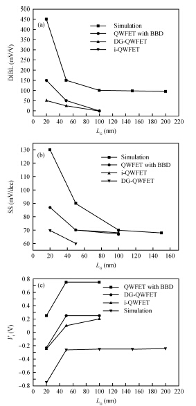
An indium antimonide based QWFET (quantum well field effect transistor) with the gate length down to 50 nm has been designed and investigated for the first time for L-band radar applications at 230 GHz. QWFETs are designed at the high performance node of the International Technology Road Map for Semiconductors (ITRS) requirements of drive current (Semiconductor Industry Association 2010). The performance of the device is investigated using the SYNOPSYS CAD (TCAD) software. InSb based QWFET could be a promising device technology for very low power and ultra-high speed performance with 5-10 times low DC power dissipation.


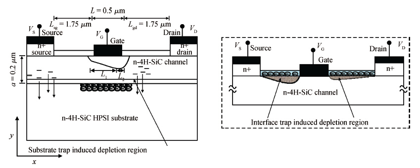
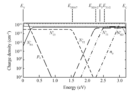
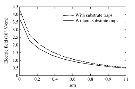
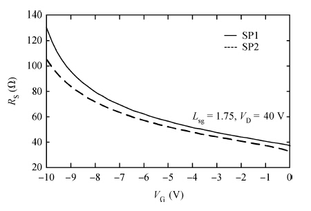
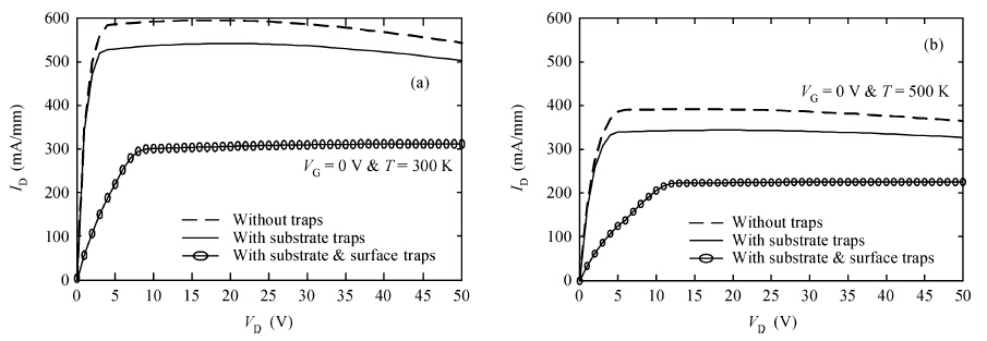
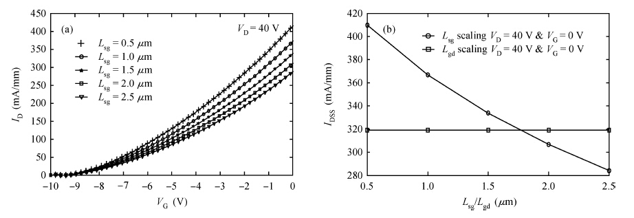
An improved analytical model for the current-voltage (I-V) characteristics of the 4H-SiC metal semiconductor field effect transistor (MESFET) on a high purity semi-insulating (HPSI) substrate with trapping and thermal effects is presented. The 4H-SiC MESFET structure includes a stack of HPSI substrates and a uniformly doped channel layer. The trapping effects include both the effect of multiple deep-level traps in the substrate and surface traps between the gate to source/drain. The self-heating effects are also incorporated to obtain the accurate and realistic nature of the analytical model. The importance of the proposed model is emphasised through the inclusion of the recent and exact nature of the traps in the 4H-SiC HPSI substrate responsible for substrate compensation. The analytical model is used to exhibit DC I-V characteristics of the device with and without trapping and thermal effects. From the results, the current degradation is observed due to the surface and substrate trapping effects and the negative conductance introduced by the self-heating effect at a high drain voltage. The calculated results are compared with reported experimental and two-dimensional simulations (Silvaco®-TCAD). The proposed model also illustrates the effectiveness of the gate-source distance scaling effect compared to the gate-drain scaling effect in optimizing 4H-SiC MESFET performance. Results demonstrate that the proposed I-V model of 4H-SiC MESFET is suitable for realizing SiC based monolithic circuits (MMICs) on HPSI substrates.


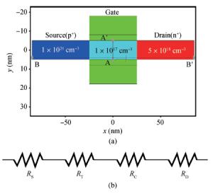
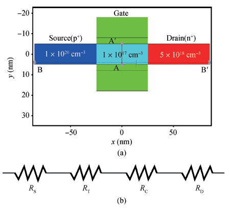
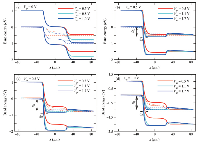
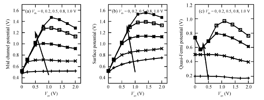
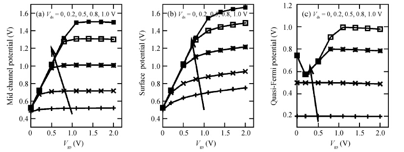
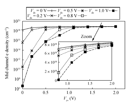
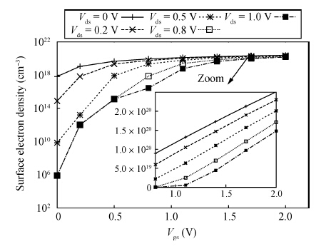
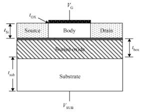
A detailed investigation carried out, with the help of extensive simulations using the TCAD device simulator Sentaurus, with the aim of achieving an understanding of the effects of variations in gate and drain potentials on the device characteristics of a silicon double-gate tunnel field effect transistor (Si-DG TFET) is reported in this paper. The investigation is mainly aimed at studying electrical properties such as the electric potential, the electron density, and the electron quasi-Fermi potential in a channel. From the simulation results, it is found that the electrical properties in the channel region of the DG TFET are different from those for a DG MOSFET. It is observed that the central channel potential of the DG TFET is not pinned to a fixed potential even after the threshold is passed (as in the case of the DG MOSFET); instead, it initially increases and later on decreases with increasing gate voltage, and this is also the behavior exhibited by the surface potential of the device. However, the drain current always increases with the applied gate voltage. It is also observed that the electron quasi-Fermi potential (eQFP) decreases as the channel potential starts to decrease, and there are hiphops in the channel eQFP for higher applied drain voltages. The channel regime resistance is also observed for higher gate length, which has a great effect on the I-V characteristics of the DG TFET device. These channel regime electrical properties will be very useful for determining the tunneling current; thus these results may have further uses in developing analytical current models.


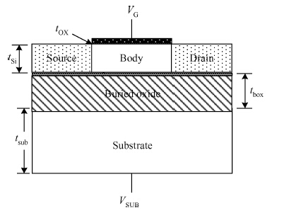
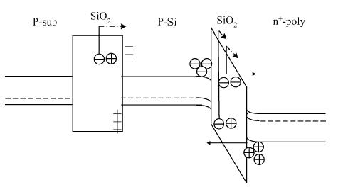
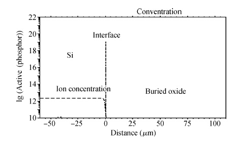
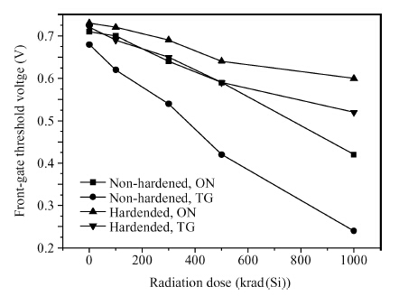
The mechanism of improving the TID radiation hardened ability of partially depleted silicon-on-insulator (SOI) devices by using the back-gate phosphorus ion implantation technology is studied. The electron traps introduced in SiO2 near back SiO2/Si interface by phosphorus ions implantation can offset positive trapped charges near the back-gate interface. The implanted high concentration phosphorus ions can greatly reduce the back-gate effect of a partially depleted SOI NMOS device, and anti-total-dose radiation ability can reach the level of 1 Mrad(Si) for experimental devices.


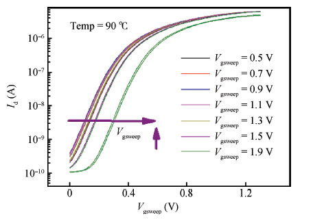
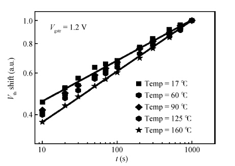
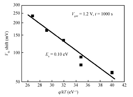
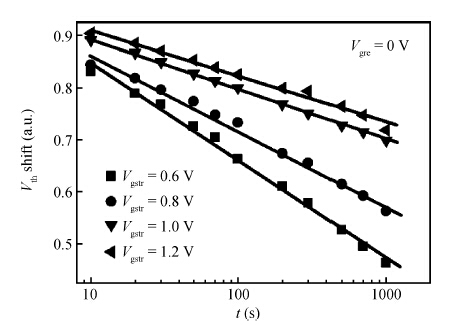
Positive bias temperature instability (PBTI) characteristics and degradation mechanisms of NMOSFET with high-k/metal gate last process have been systematically investigated. The time evolution of threshold voltage shift during PBTI stress still follows a power law. However, the exponent n decreases from 0.26 to 0.16 linearly as the gate stress voltage increases from 0.6 to 1.2 V. There is no interface state generation during stress because of the negligible sub-threshold swing change. Moreover, the activation energy is 0.1 eV, which implies that electrons directly tunnel into high-k bulk and are trapped by pre-existing traps resulting into PBTI degradation. During recovery the threshold voltage shift is linear in lgt, and a mathematical model is proposed to express threshold voltage shift.


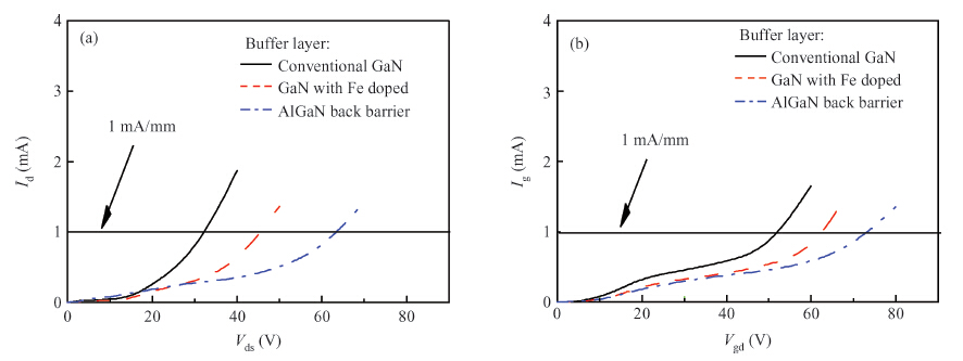
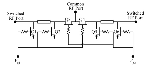
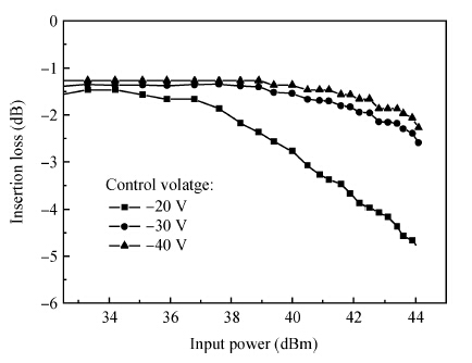
0.25 μm GaN HEMT with AlGaN back barrier for high power switch application has been presented. By introducing AlGaN back barrier, the buffer layer breakdown voltage for the metal-organic chemical vapor deposited AlGaN/GaN hetero-structure on 3-inch SiC substrate showed a considerable increment, which was nearly 4× and 2× of that for the conventional GaN buffer layer and GaN buffer layer with Fe doped, respectively. GaN switch HEMTs with source to drain spacing of 2, 2.5, 3, 3.5 and 4 μm were fabricated on the AlGaN/GaN epitaxial material with AlGaN back barrier and estimated off state power handling for the GaN switch HEMTs were 25.0, 46.2, 64.0, 79.2, and 88.4 W, respectively. A demonstrator DC-12 GHz GaN SPDT MMIC switch was designed in reflective series-shunt-shunt configuration based on the GaN HEMT, with a source to drain spacing of 2.5 μm. The developed SPDT MMIC switch showed a maximum insertion loss of 1.0 dB and a minimum isolation of 30 dB at a frequency range of DC-12 GHz. A power handling capability of 44.1 dBm was achieved at 10 GHz for the MMIC switch with continuous wave power compression measurement.


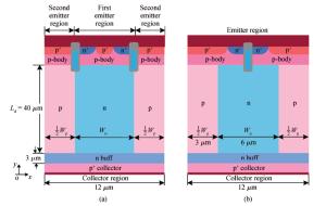
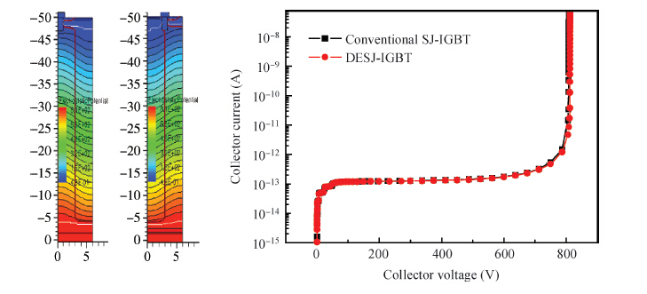
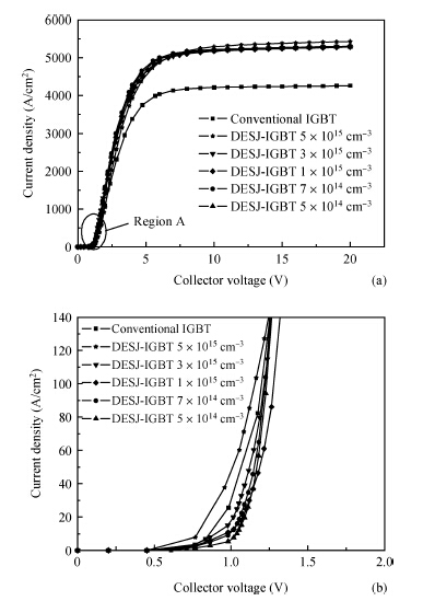
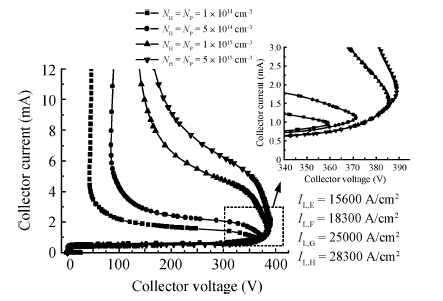
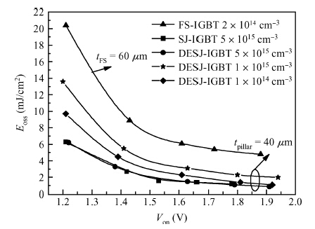
An improved trench gate super-junction insulated-gate bipolar transistor is presented. The improved structure contains two emitter regions. The first emitter region of the device works as the conventional structure, which can absorb both the electron current and hole current. The second emitter on the top of the p-pillar acts as the hole current diverter, leading to an improved latch-up capability without sacrificing the off-state breakdown voltage (BV) and turn-off loss. The simulation shows that the latch-up limit of the SJ-IGBT increases from 15000 to 28300 A/cm2 at VGE = 10 V, the BV is 810 V, and the turn off loss is 6.5 mJ/cm2 at Von = 1.2 V.


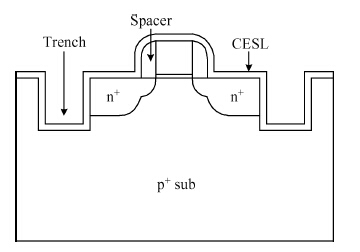
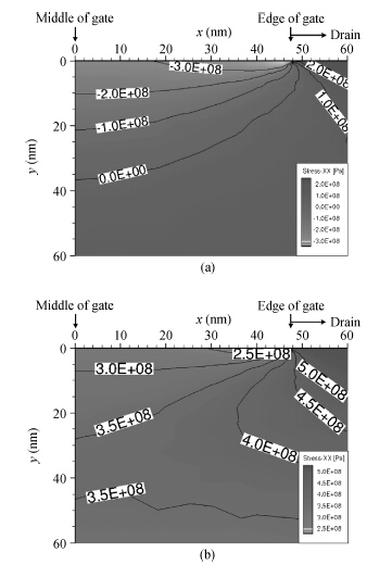
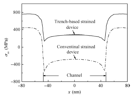
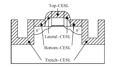
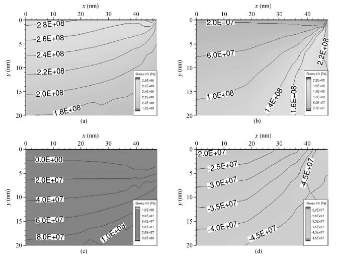
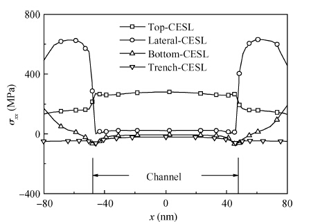
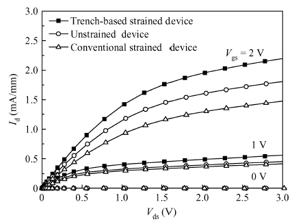
A stress modulation technology using a trench-based structure for strained NMOSFET is reported in this paper. With this technology, NMOSFET can be improved by a compressive contact etch stop layer (CESL), whereas the traditional CESL-strained NMOSFET requires a tensile one. To confirm this idea, a 95-nm-gate device with a-2.5 GPa strained CESL is simulated to investigate the effects of the trench-based structure on channel stress. It is demonstrated that the average longitudinal channel stress is transformed from-333 into 256 MPa, which leads to a significant improvement of the device's I-V performance. For strained CMOS, this approach provides a potential alternative besides dual stress liner technology.


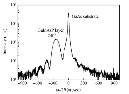
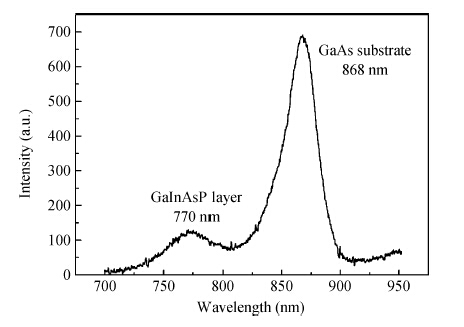
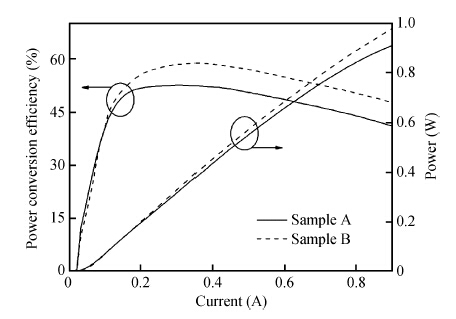
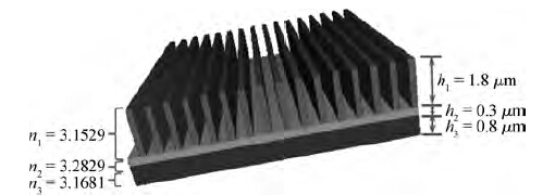
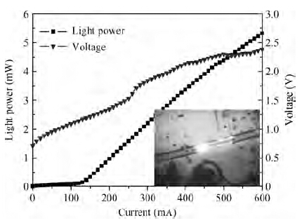
GaInAsP layers and GaAsP/ (Al) GaInP laser diodes (LDs) have been grown on GaAs substrates by metalorganic chemical vapor deposition. The GaInAsP layer, which is lattice matched to GaAs, has an intermediate band gap between Ga0.5In0.5P and GaAs. The GaInP/GaAs heterojunction spikes, especially in the valence band, can be suppressed by introducing this thin GaInAsP layer into the heterostructure interface. The 808 nm GaAsP/ (Al) GaInP LDs with GaInAsP intermediate layer show a reduced operating voltage compared to the conventional LDs with abrupt GaInP/GaAs interface due to the enhanced hole injection. As a result, the power conversion efficiency is improved from 52% to 60% at 350 mW output power. At high current injection, the LD with GaInAsP intermediate layer has higher light power owing to the decreased joule heating.


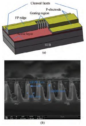
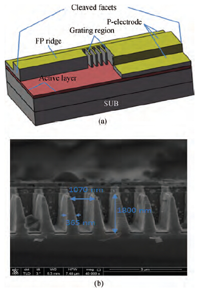
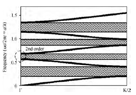
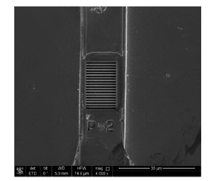
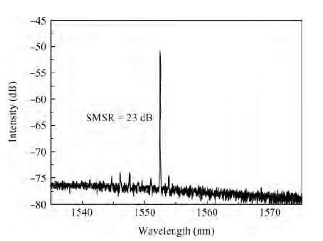
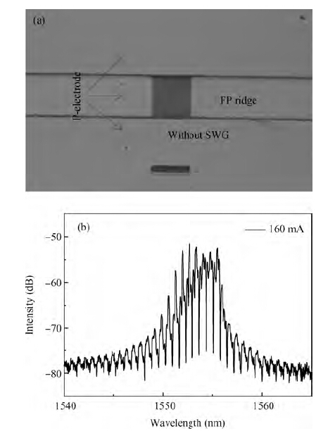
We report a novel lateral cavity surface emitting laser based on sub-wavelength high-index-contrast grating with in-plane resonance and surface-normal emission. The device is fabricated on a simple commercial wafer without the distributed Bragg reflector and it needs no wafer bonding. It exhibits a side mode suppression ratio of 23.0 dB and a high output power of 5.32 mW at 1552.44 nm. The specific single mode lasing agrees well with the band edge mode calculation of the grating. In 3D simulation, we observe obvious light output from the grating.


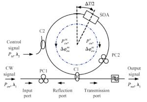
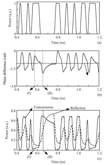
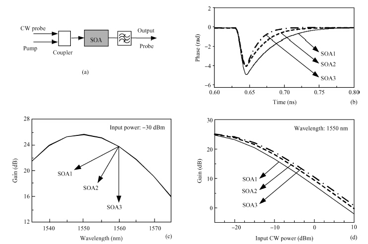
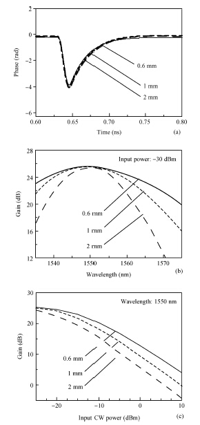
We investigated the all-optical wavelength conversion technique for non-return-to-zero (NRZ) signals based on a Sagnac loop interferometer using an SOA. For the wavelength conversion of the NRZ signal at and above 40 Gbit/s, we used an in-house numerical SOA model to analyze the influence of the SOA carrier characteristics and the SOA length on the performance of the Sagnac loop. We found that the SOA carrier recovery time should be between 2 and 3 times of one bit duration in order to get optimum NRZ wavelength conversion. In addition to the carrier recovery time requirement, SOAs with a shorter physical length are preferred to be used in the Sagnac interferometer.


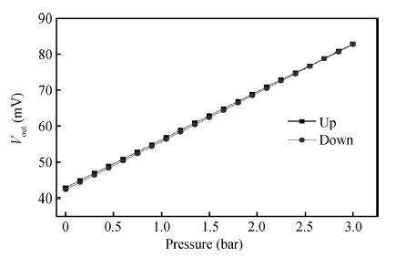
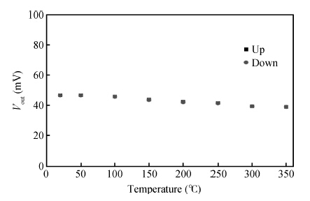
The silicon on insulator (SOI) high temperature pressure sensor is a novel pressure sensor with high-performance and high-quality. A structure of a SOI high-temperature pressure sensor is presented in this paper. The key factors including doping concentration and power are analyzed. The process of the sensor is designed with the critical process parameters set appropriately. The test result at room temperature and high temperature shows that nonlinear error below is 0.1%, and hysteresis is less than 0.5%. High temperature measuring results show that the sensor can be used for from room temperature to 350 ℃ in harsh environments. It offers a reference for the development of high temperature piezoresistive pressure sensors.


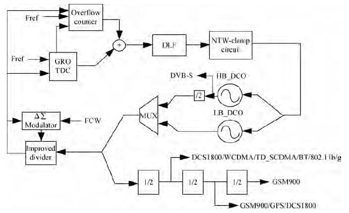
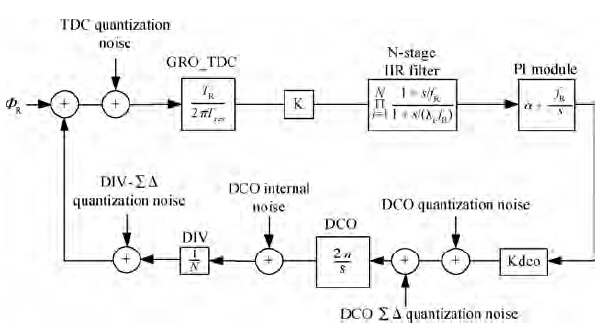
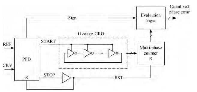
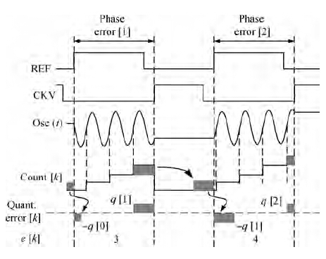
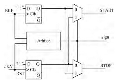
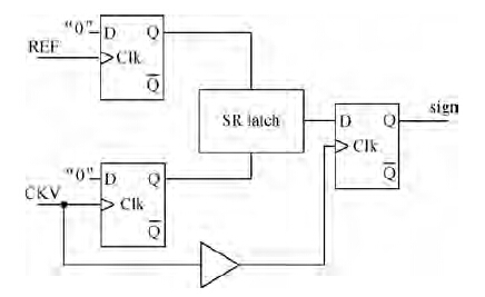
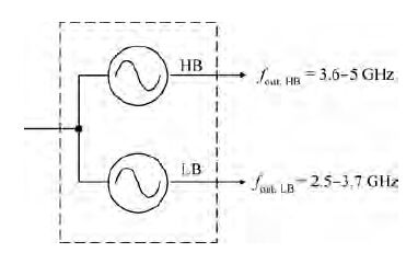
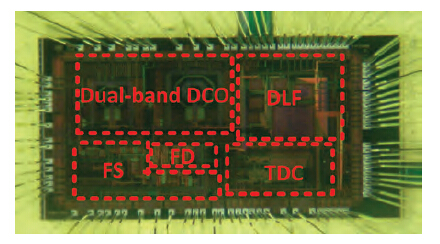
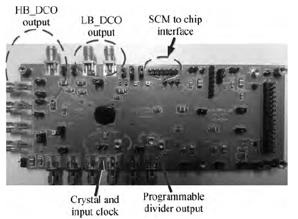
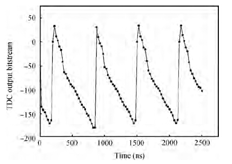
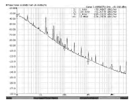
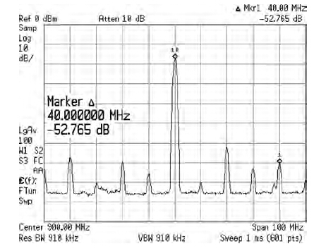
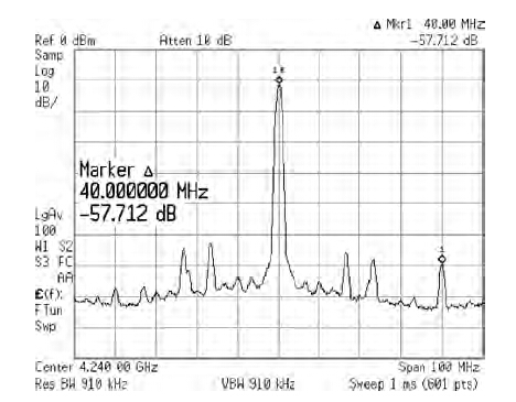
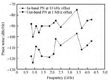
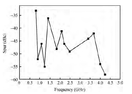
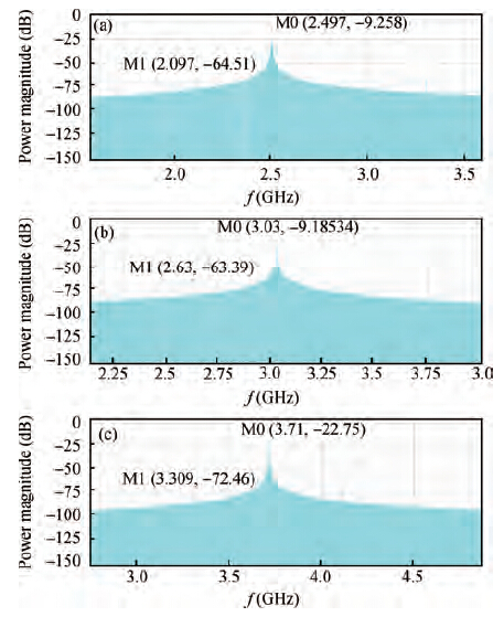
A 0.8-4.2 GHz monolithic all-digital PLL based frequency synthesizer for wireless communications is successfully realized by the 130 nm CMOS process. A series of novel methods are proposed in this paper. Two band DCOs with high frequency resolution are utilized to cover the frequency band of interest, which is as wide as 2.5 to 5 GHz. An overflow counter is proposed to prevent the "pulse-swallowing" phenomenon so as to significantly reduce the locking time. A NTW-clamp digital module is also proposed to prevent the overflow of the loop control word. A modified programmable divider is presented to prevent the failure operation at the boundary. The measurement results show that the output frequency range of this frequency synthesizer is 0.8-4.2 GHz. The locking time achieves a reduction of 84% at 2.68 GHz. The best in-band and out-band phase noise performances have reached-100 dBc/Hz, and-125 dBc/Hz respectively. The lowest reference spur is-58 dBc.


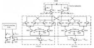
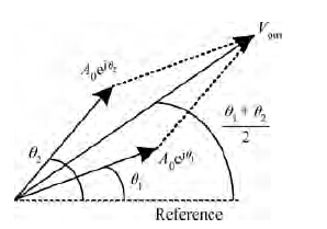
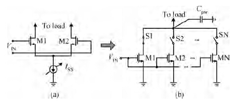
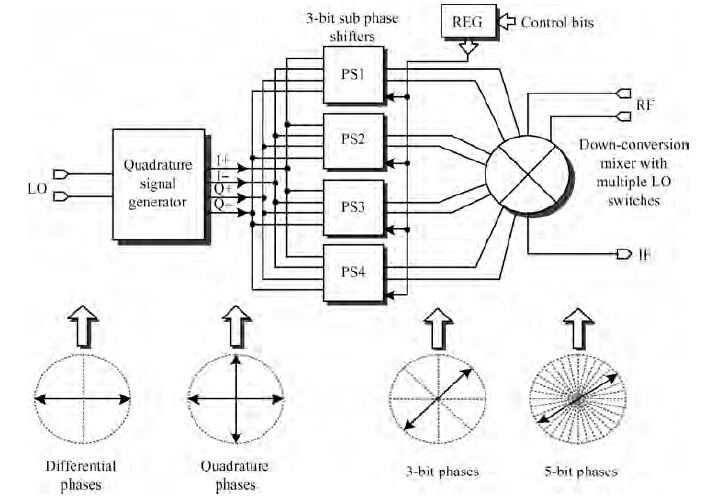
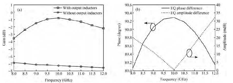
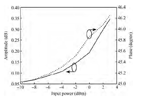
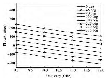
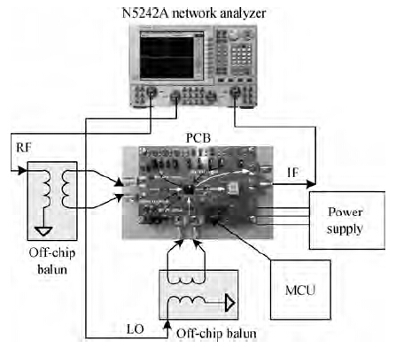
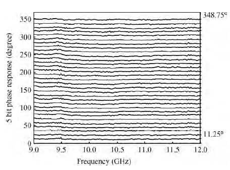
This paper presents a 5-bit active LO phase shifter with a new vector sum method for 9-12 GHz applications. The 5-bit phase shifter is composed of four 3-bit sub phase shifters by adopting the new vector sum method, which reduces the requirements on the resolution of the variable gain amplifier (VGA). The variable gain function is realized by switch on/off parallel input transistor pairs rather than changing the bias current of the VGA, which avoids the linearity variation and drain-source voltage variation existing in the quadrature vector sum active phase shifter. The 5-bit active LO phase shifter is fabricated in TSMC 0.13 μm CMOS technology. The measured results show that the phase shifter achieves 5-bit phase shift accuracy. The average conversion gain for 32 phase states is-0.5 to 7 dB from 9 to 12 GHz. The RMS gain error and the RMS phase error are smaller than 0.8 dB and 4° respectively. The current consumption is 27.7 mA from a 1.2 V supply voltage.


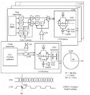
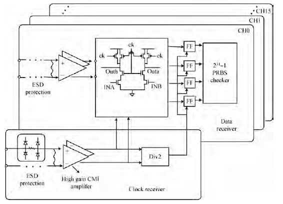
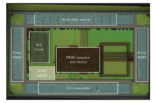
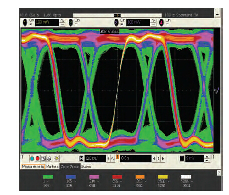
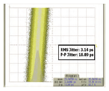
This paper describes a 65 nm 16-bit parallel transceiver IP macro, whose rate is 3 Gb/s with a 5 pF load including the HBM 2000 V ESD protection. Equalizers and clock data recovery modules, CRC checkers and 8 b/10 b encoders are not added in the design for reducing the latency, and the whole latency is 7 ns without cables. Since the transceiver has many robust features including a process, voltage and temperature independent phase-locked loop with calibrations, the low skew differential clock tree, and a stable current mode driver with common mode feedback, the transceiver can work properly at different process corners and extreme temperatures, and also can tolerate 20% power supply variations. The transceiver can be applied for the interface of sub-100 nm high performance processors, which require low latency and high stability. The transceiver shows a bitter error ratio of less than 10-15 at 3 Gbps.

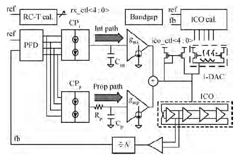


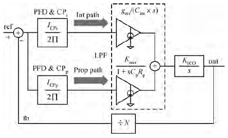


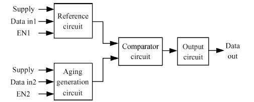
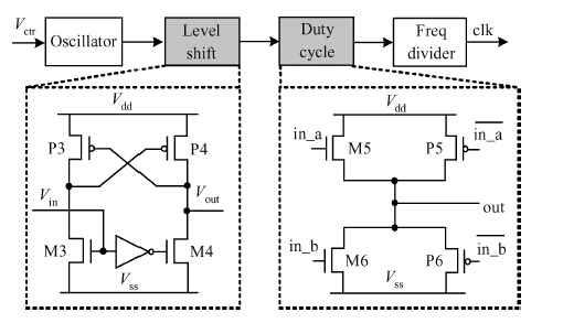
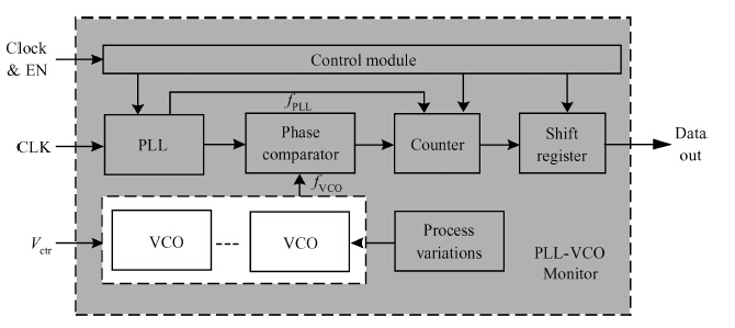
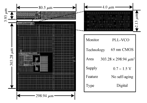
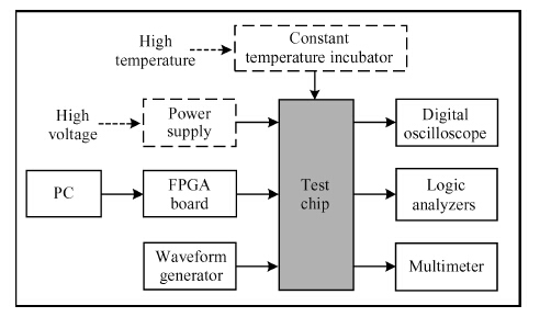
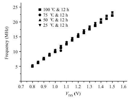
As the manufacturing process is scaled down to the nanoscale, the aging phenomenon significantly affects the reliability and lifetime of integrated circuits. Consequently, the precise measurement of digital CMOS aging is a key aspect of nanoscale aging tolerant circuit design. This paper proposes a high accuracy digital aging monitor using phase-locked loop and voltage-controlled oscillator (PLL-VCO) circuit. The proposed monitor eliminates the circuit self-aging effect for the characteristic of PLL, whose frequency has no relationship with circuit aging phenomenon. The PLL-VCO monitor is implemented in TSMC low power 65 nm CMOS technology, and its area occupies 303.28 × 298.94 μm2. After accelerating aging tests, the experimental results show that PLL-VCO monitor improves accuracy about high temperature by 2.4% and high voltage by 18.7%.


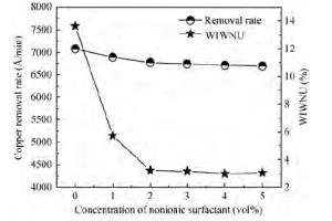
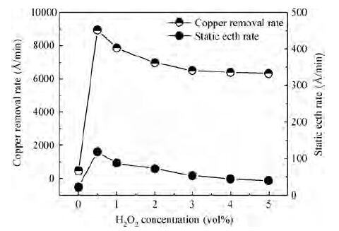
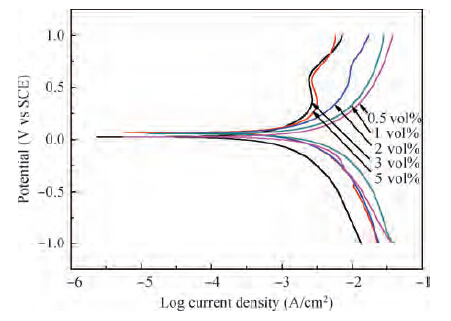
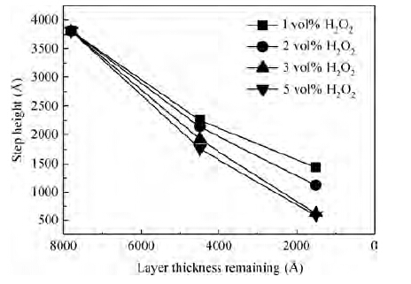
For improving the polishing performance, in this article, the roles of a nonionic surfactant (Fatty alcohol polyoxyethylene ether) and H2O2 were investigated in the chemical mechanical planarization process, respectively. Firstly, the effects of the nonionic surfactant on the within-wafer non-uniformity (WIWNU) and the surface roughness were mainly analyzed. In addition, the passivation ability of the slurry, which had no addition of BTA, was also discussed from the viewpoint of the static etch rate, electrochemical curve and residual step height under different concentrations of H2O2. The experimental results distinctly revealed that the nonionic surfactant introduced in the slurry improved the WIWNU and surface roughness, and that a 2 vol% was considered as an appropriate concentration relatively. When the concentration of H2O2 surpasses 3 vol%, the slurry will possess a relatively preferable passivation ability, which can effectively decrease the step height and contribute to acquiring a flat and smooth surface. Hence, based on the result of these experiments, the influences of the nonionic surfactant and H2O2 are further understood, which means the properties of slurry can be improved.


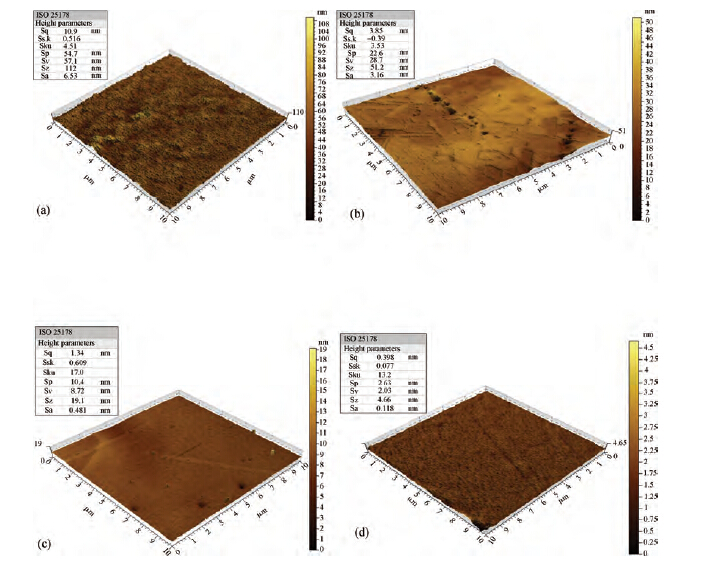

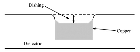
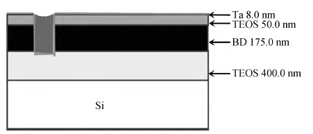
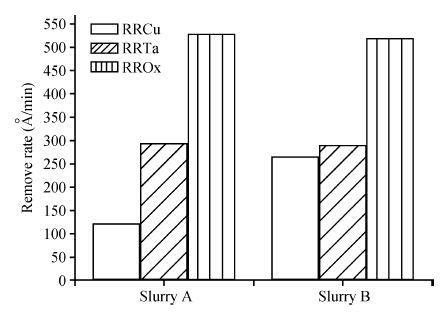
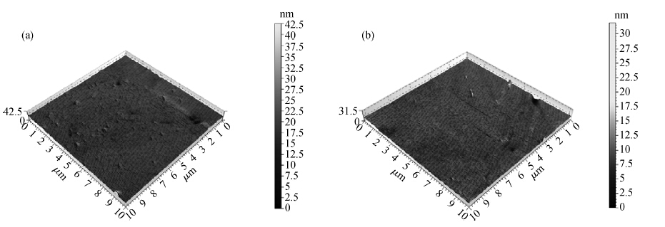
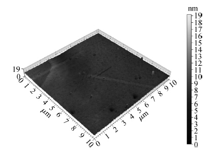
To strengthen the device performance with the pattern wafer by enhancing the Cu polishing rate and improve the surface roughness with the Cu lines, a new weakly alkaline chelating agent with a barrier slurry is developed to meet the process demand of the advanced barrier chemical mechanical planarization (CMP). This new chelating agent has a stronger chelating ability and a lower pH value than the previous generation-FA/O I chelating agent researched before. Without an unstable oxidant agent added in the polishing slurry, it is difficult to enhance the copper polishing rate during the barrier CMP. The stronger chelating ability of the new chelating agent could increase the copper polishing rate along with controlling the Cu/Ta/TEOS removal rate selectivity to meet the requirements of the IC fabrication process. Thus it has solved the problem of excessive roughness due to the lower polishing rate, avoiding reducing the device performance with the pattern wafer. The new chelating agent with its lower pH value could make it possible to protect the low-k dielectric under the barrier layer from structurally breaking. The CMP experiment was performed on the 12 inch MIT 854 pattern wafers with the barrier slurry containing the new weakly alkaline chelating agent. By the DOE optimization, the results indicate that as the new chelating agent concentration in the slurry was up to 2.5 mL/L, the copper polishing rate is about 31.082 nm/min. Meanwhile, the wafer surface has a rather low roughness value of 0.693 nm (10 × 10 μm), the correction ability with the above slurry is adapted to the next generation barrier CMP and the k value of the low-k dielectric seems to have no k-shift. All the results presented show that the new weakly alkaline chelating agent with its superior performance can be used for the advanced barrier CMP.