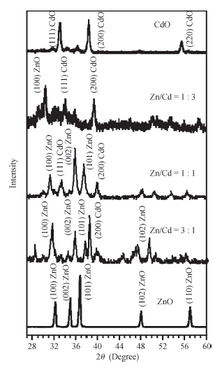
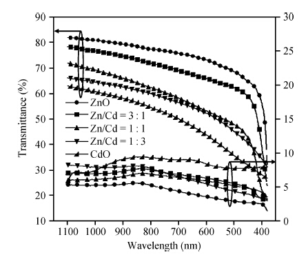
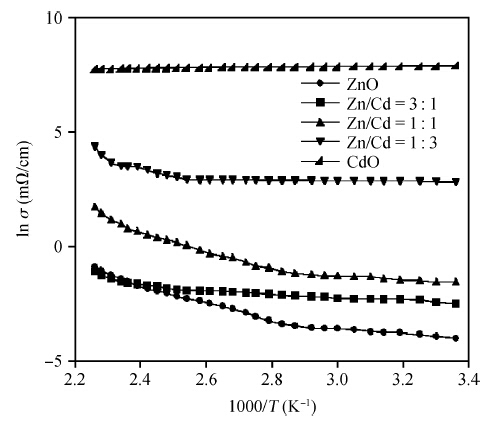
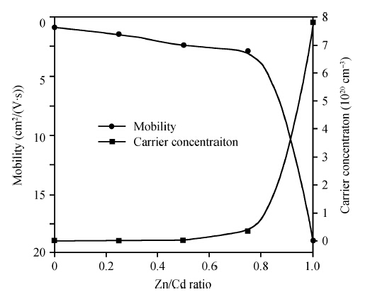
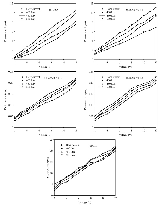
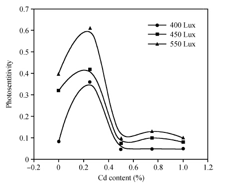
A series of ZnO-CdO thin films of different molar ratios of Zn and Cd have been deposited on glass substrate at substrate temperature ~ 360 ℃ by the spray pyrolysis technique at an ambient atmosphere. X-ray diffraction (XRD) studies confirmed the polycrystalline nature of the film and modulated crystal structures of wurtzite (ZnO) and cubic (CdO) are formed. The evaluated lattice parameters, and crystallite size are consistent with literature. Dislocation density and strain increased in the film as the grain sizes of ZnO and CdO are decreased. The band gap energy varies from 3.20 to 2.21 eV depending on the Zn/Cd ratios in the film. An incident photon intensity dependent I-V study confirmed that the films are highly photosensitive. Current increased with the increase of the intensity of the light beam. The optical conductivity and the optical constants, such as extinction coefficient, refractive index and complex dielectric constants are evaluated from transmittance and reflectance spectra of the films and these parameters are found to be sensitive to photon energy and displayed intermediate optical properties between ZnO and CdO, making it preferable for applications as the buffer and window layers in solar cells.


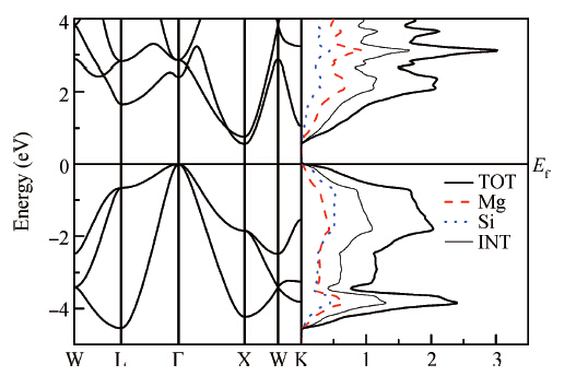
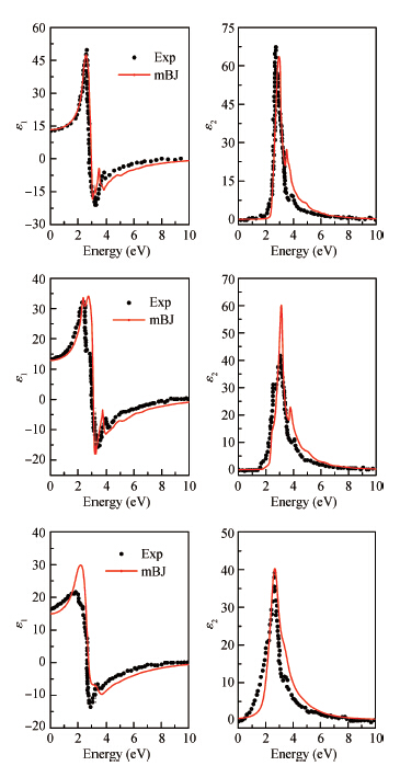
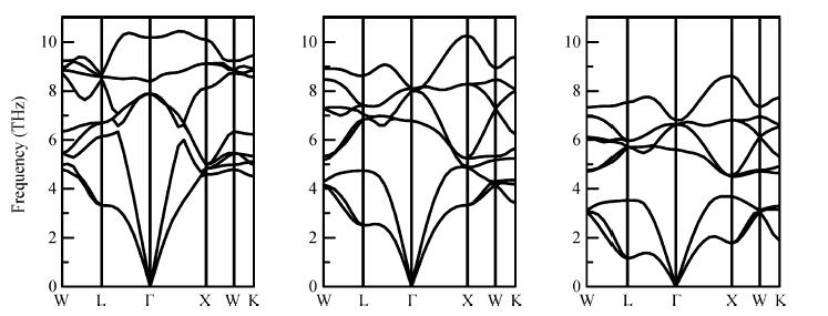
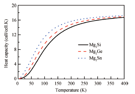
The electronic structures of Mg2X (X = Si, Ge, Sn) have been calculated by using generalized gradient approximation, various screened hybrid functionals, as well as Tran and Blaha's modified Becke and Johnson exchange potential. It was found that the Tran and Blaha's modified Becke and Johnson exchange potential provides a more realistic description of the electronic structures and the optical properties of Mg2X (X = Si, Ge, Sn) than else exchange-correlation potential, and the theoretical gaps and dielectric functions of Mg2X (X = Si, Ge, Sn) are quite compatible with the experimental data. The elastic properties of Mg2X (X = Si, Ge, Sn) have also been studied in detail with the generalized gradient approximation, including bulk modulus, shear modulus, Young's modulus, Poisson's ratio, sound velocities, and Debye temperature. The phonon dispersions of Mg2X (X = Si, Ge, Sn) have been calculated within the generalized gradient approximation, suggesting no structural instability, and the measurable phonon heat capacity as a function of the temperature has been also calculated.

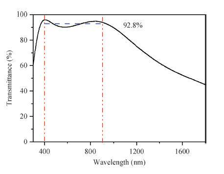
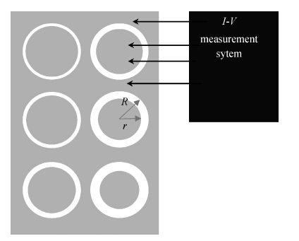
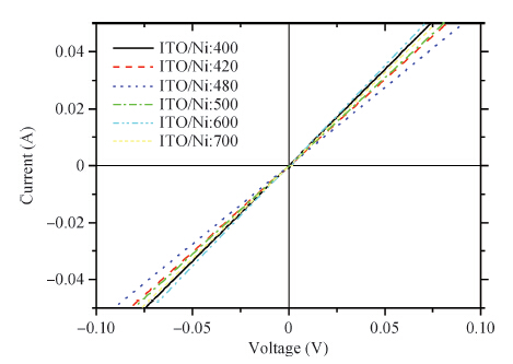
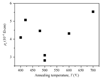
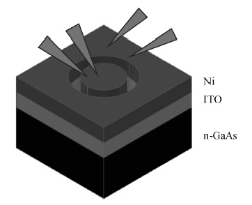
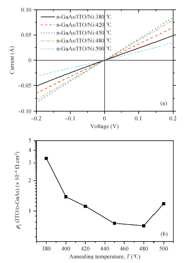
We report the specific contact resistance for ITO with both metal and a semiconductor. Good quality ITO was deposited by electron beam evaporation with the resistivity of 2.32 × 10⁻⁴ Ω ·cm and an averaged transmittance of 92.8% in the visible light region. The circular transmission line model (c-TLM) method was used to evaluate and compare the properties of the ITO/metal and ITO/semiconductor ohmic contacts. The lowest specific contact resistance of the ITO/Ni is 2.81 × 10⁻⁶ Ω ·cm2, while that of ITO/n-GaAs is 7 × 10⁻⁵ Ω ·cm2. This is the best ohmic contact between ITO and n-GaAs ever reported. These results suggest that good quality ITO has strong potential to be used to realize highly efficient solar cells.


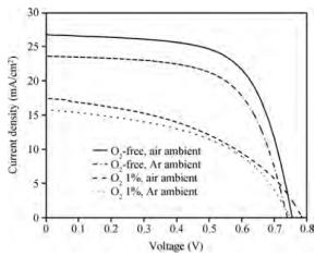
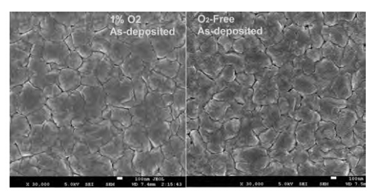
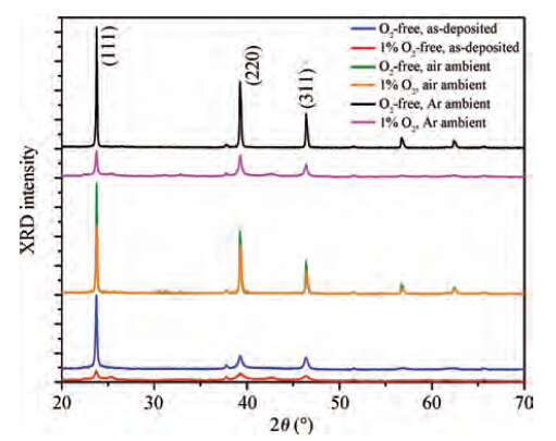
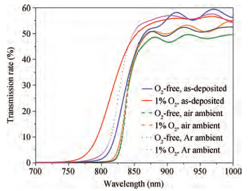
1% oxygen is incorporated into both CdS and CdTe layers through RF sputtering of CdS/CdTe thin film solar cells. The optical and electrical parameters of the oxygenated and O2-free devices are compared after CdCl2 treatment and annealing in ambient Ar and/or air. The effects of ambient annealing on the electrical and optical properties of the films are investigated using current-voltage characterization, field emission scanning electron microscopy, X-ray diffraction, and optical transmission spectroscopy. The 1% oxygen content can slightly increase the grain size while the crystallinity does not change. Annealing in ambient Ar can increase the transmission rate of the oxygenated devices.

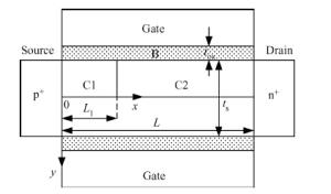
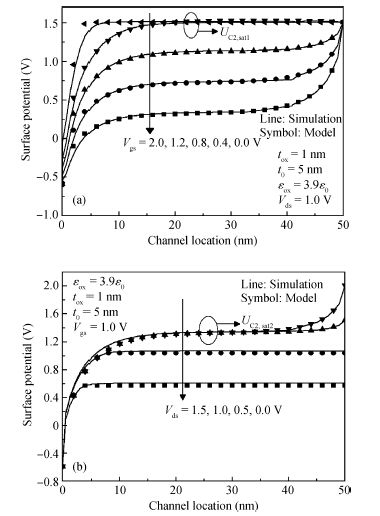
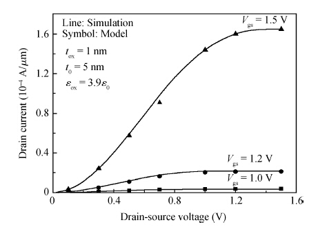
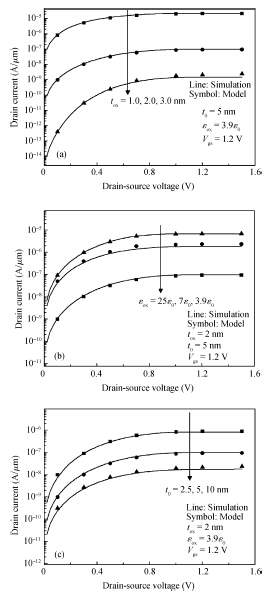
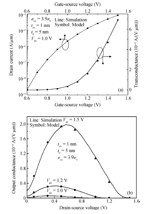
A 2-D semi-analytical model of double gate (DG) tunneling field-effect transistor (TFET) is proposed. By aid of introducing two rectangular sources located in the gate dielectric layer and the channel, the 2-D Poisson equation is solved by using a semi-analytical method combined with an eigenfunction expansion method. The expression of the surface potential is obtained, which is a special function for the infinite series expressions. The influence of the mobile charges on the potential profile is taken into account in the proposed model. On the basis of the potential profile, the shortest tunneling length and the average electrical field can be derived, and the drain current is then constructed by using Kane's model. In particular, the changes of the tunneling parameters Ak and Bk influenced by the drain-source voltage are also incorporated in the predicted model. The proposed model shows a good agreement with TCAD simulation results under different drain-source voltages, silicon film thicknesses, gate dielectric layer thicknesses, and gate dielectric layer constants. Therefore, it is useful to optimize the DG TFET and this provides a physical insight for circuit level design.


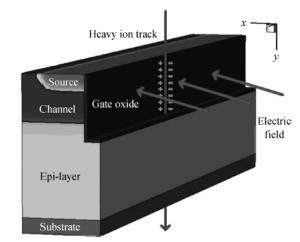
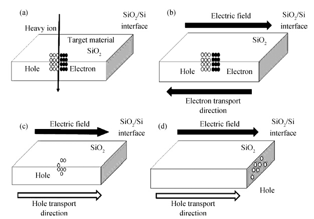
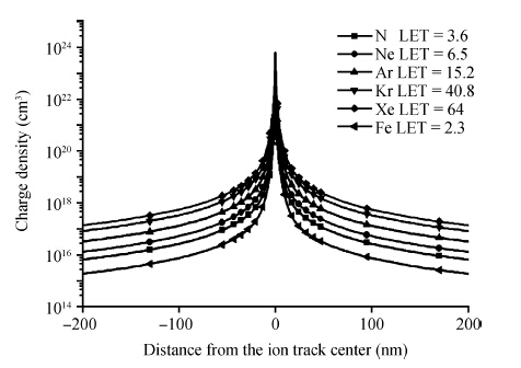
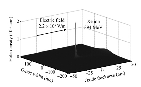
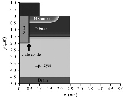
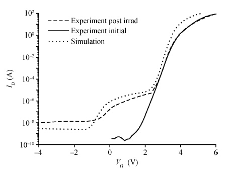
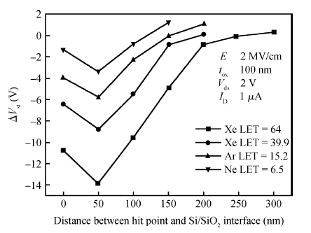
It was demonstrated that heavy ions can induce large current-voltage (I-V) characteristics shift in commercial trench power MOSFETs, named single event microdose effect (SE-microdose effect). A model is presented to describe this effect. This model calculates the charge deposition by a single heavy ion hitting oxide and the subsequent charge transport under an electric field. Holes deposited at the SiO2/Si interface by a Xe ion are calculated by using this model. The calculated results were then used in Sentaurus TCAD software to simulate a trench power MOSFET's I-V curve shift after a Xe ion has hit it. The simulation results are consistent with the related experiment's data. In the end, several factors which affect the SE-microdose effect in trench power MOSFETs are investigated by using this model.


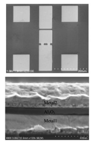
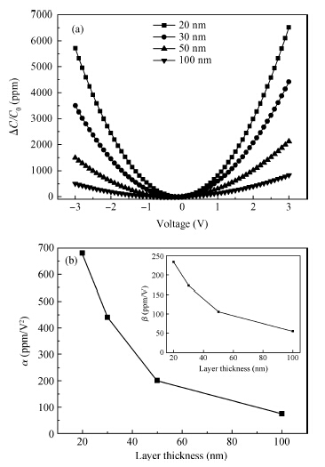
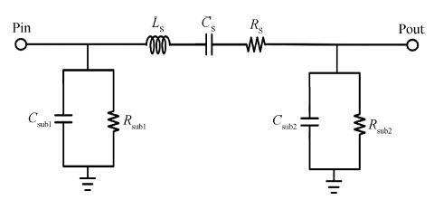
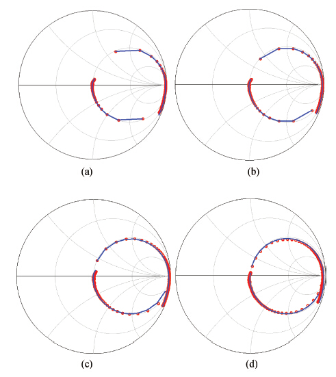
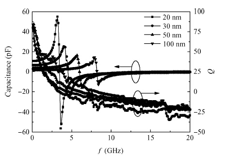
The impact of various thicknesses of Al2O3 metal-insulator-metal (MIM) capacitors on direct current and radio frequency (RF) characteristics is investigated. For 20 nm Al2O3, the fabricated capacitor exhibits a high capacitance density of 3850 pF/mm2 and acceptable voltage coefficients of capacitance of 681 ppm/V2 at 1 MHz. An outstanding VCC-α of 74 ppm/V2 at 1 MHz, resonance frequency of 8.2 GHz and Q factor of 41 at 2 GHz are obtained by 100 nm Al2O3 MIM capacitors. High-performance MIM capacitors using GaAs process and atomic layer deposition Al2O3 could be very promising candidates for GaAs RFIC applications.


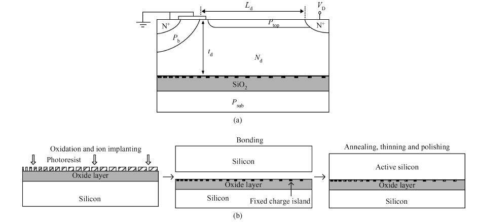
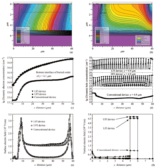
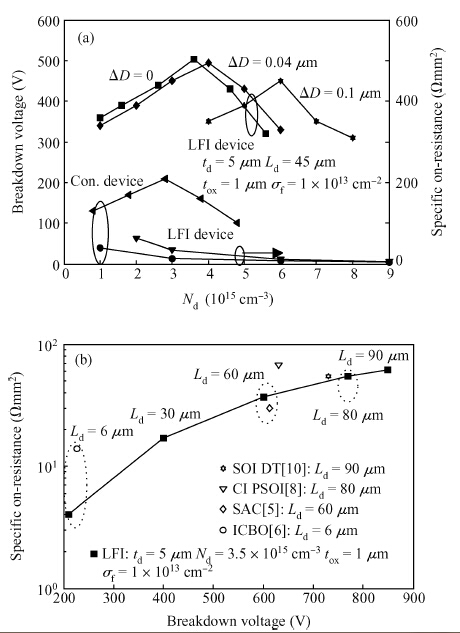
A new high-voltage LDMOS with linearly-distanced fixed charge islands is proposed (LFI LDMOS). A lot of linearly-distanced fixed charge islands are introduced by implanting the Cs or I ion into the buried oxide layer and dynamic holes are attracted and accumulated, which is crucial to enhance the electric field of the buried oxide and the vertical breakdown voltage. The surface electric field is improved by increasing the distance between two adjacent fixed charge islands from source to drain, which lead to the higher concentration of the drift region and a lower on-resistance. The numerical results indicate that the breakdown voltage of 500 V with Ld = 45 μm is obtained in the proposed device in comparison to 209 V of conventional LDMOS, while maintaining low on-resistance.


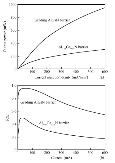
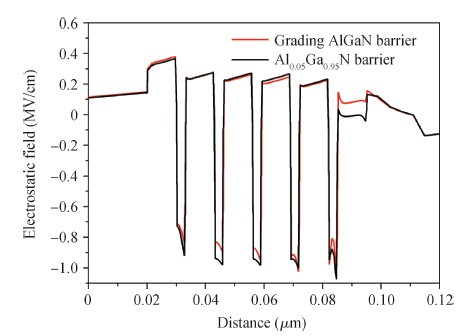
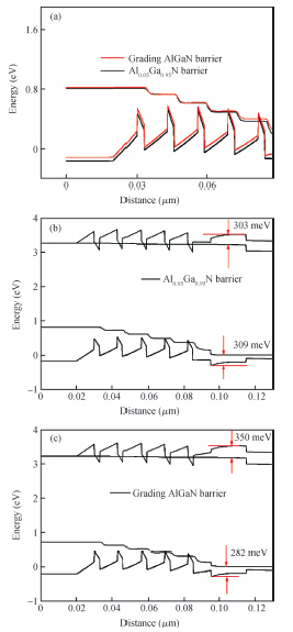
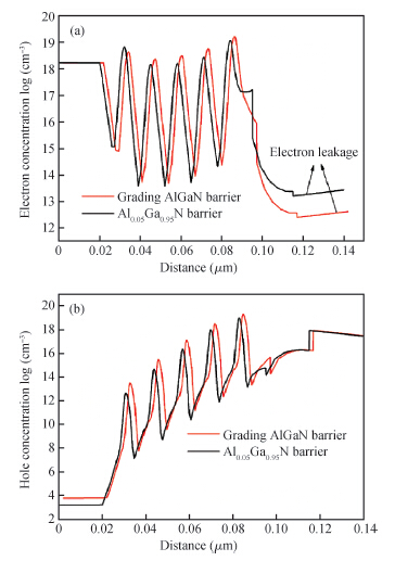
The characteristics of nitride-based blue light-emitting diodes (LEDs) with AlGaN composition-graded barriers are analyzed numerically. The carrier concentrations in the quantum wells (QWs), the energy band diagrams, the electrostatic fields, and the light output power are investigated by APSYS software. The simulation results show that the LED with AlGaN composition-graded barriers has a better performance than its AlGaN/InGaN counterpart owing to the increase of hole injection and the enhancement of electron confinement. The simulation results also suggest that the output power is enhanced significantly and the efficiency droop is markedly improved when the AlGaN barriers are replaced by AlGaN composition-graded barriers.
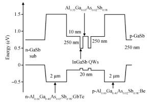
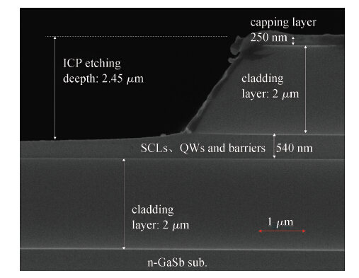
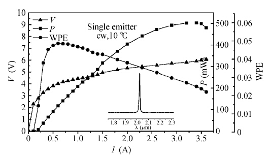
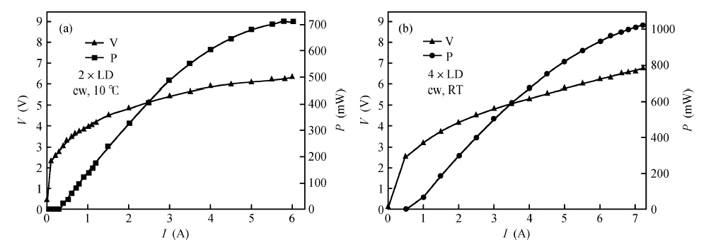
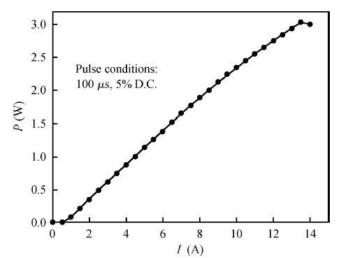
2 μ m AlGaAsSb/InGaSb type-I quantum-well high-power laser diodes (LDs) are grown using molecular beam epitaxy. Stripe-type waveguide single LD (single emitter) and array LD (four emitters) devices without facet coatings are fabricated. For the single LDs (single emitter) device, the maximum output power under continuous wave (CW) operation is 0.5 W at 10 ℃ with a threshold current density of 150 A/cm2 and a slope efficiency of 0.17 W/A, the output powers under the pulse mode in the 5% duty cycles are much higher, up to 0.98 W. For the array LD devices, the maximum output powers are 1.02 W under the CW mode and 3.03 W under the pulse mode at room temperature.


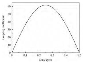
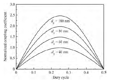
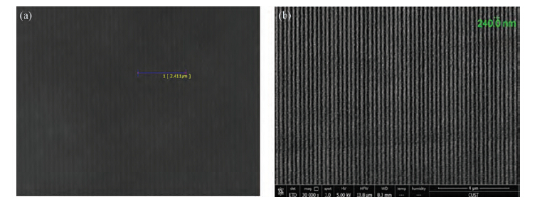
The second-order Bragg grating structure of an 808 nm distributed feedback semiconductor laser diode was designed and optimized. The grating with a period of 240 nm was fabricated on GaAs substrate by holographic photolithography and wet etching. Images of optical microscopy, scanning electron microscopy and atomic force microscopy show that the grating has a period of 240 nm, duty cycle of 0.25, depth of 80 nm, with perfect surface morphology, good fringe continuity and uniformity.

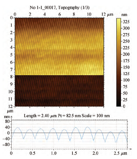

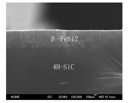
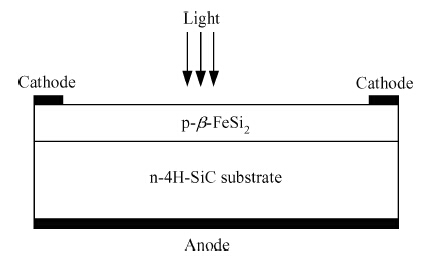
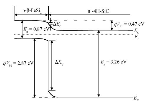
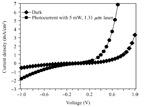
We give the first report on the experimental investigation of a p-β -FeSi2/n-4H-SiC heterojunction. A p-β -FeSi2/n-4H-SiC heterojunction near-infrared photodiode was fabricated on 4H-SiC substrate by magnetron sputtering and rapid thermal annealing (RTA). Sharp film-substrate interfaces were confirmed by scanning electron microscopy (SEM). The current density-voltage and photoresponse characteristics were measured. The measurements showed that the device exhibited good rectifying properties. The photocurrent density was about 1.82 mA/cm2 at a bias voltage of -1 V under illumination by a 5 mW, 1.31 μ m laser, and the dark current density was approximately 0.537 mA/cm2. The detectivity was estimated to be 8.8 × 10⁹ cmHz1/2/W at 1.31 μ m. All of the measurements were made at room temperature. The results suggest that the p-β -FeSi2/n-4H-SiC heterojunctions can be used as near-infrared photodiodes that are applicable to optically-activated SiC-based devices.
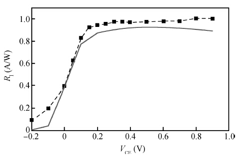
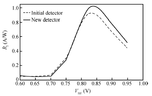
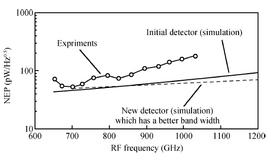
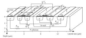
In order to improve the performance of a pre-designed direct conversion terahertz detector which is implemented in a 0.25 μ m-SiGe-BiCMOS process, we propose some slight modifications in the bipolar section of the SiGe device physical design. Comparison of our new proposed device and the previously reported device is done by SILVACO TCAD software simulation and we have used previous experimentally reported data to confirm our software simulations. Our proposed modifications in device structural design show a present device responsivity improvement of about 10% from 1 to 1.1 A/W while the bandwidth improvement is about 218 GHz. The minimum noise equivalent power at detector output is increased by about 14.3% and finally power consumption per pixel at the maximum responsivity is decreased by about 5%.


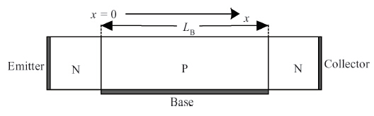
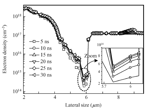
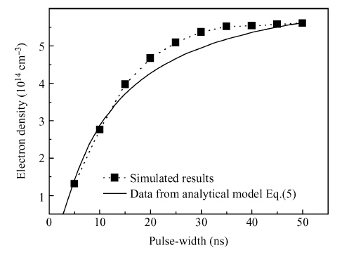
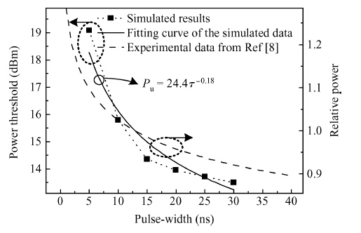
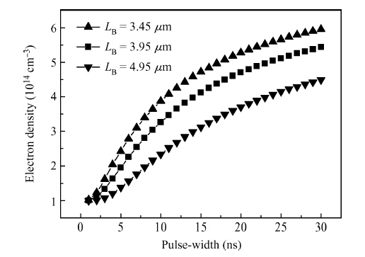
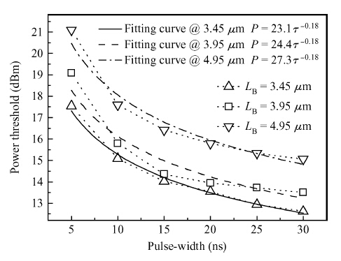
We derive analytical models of the excess carrier density distribution and the HPM (high-power microwave) upset susceptibility with dependence of pulse-width, which are validated by the simulated results and experimental data. Mechanism analysis and model derivation verify that the excess carriers dominate the current amplification process of the latch-up. Our results reveal that the excess carrier density distribution in P-substrate behaves as pulse-width dependence. The HPM upset voltage threshold Vp decreases with the incremental pulse-width, while there is an inflection point which is caused because the excess carrier accumulation in the P-substrate will be suppressed over time. For the first time, the physical essence of the HPM pulse-width upset effect is proposed to be the excess carrier accumulation effect. Validation concludes that the Vp model is capable of giving a reliable and accurate prediction to the HPM upset susceptibility of a CMOS inverter, which simultaneously considers technology information, ambient temperature, and layout parameters. From the model, the layout parameter LB has been demonstrated to have a significant impact on the pulse-width upset effect: a CMOS inverter with minor LB is more susceptible to HPM, which enables us to put forward hardening measures for inverters that are immune from the HPM upset.


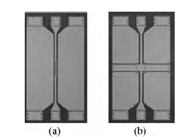
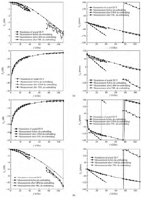
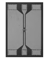
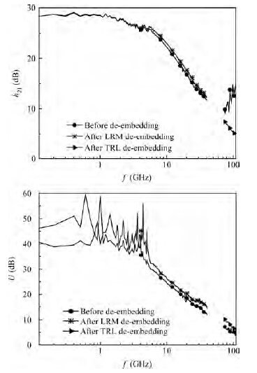
On-wafer S-parameter de-embedding techniques from 0.1 to 110 GHz are researched. The solving results of thru-reflect-line (TRL) and line-reflect-match (LRM) de-embedding algorithms, when the input and output ports are asymmetric, are given. The de-embedding standards of TRL and LRM are designed on an InP substrate. The validity of the de-embedding results is demonstrated through two passive components, and the accuracy of TRL and LRM de-embedding techniques is compared from 0.1 to 110 GHz. By utilizing an LRM technique in 0.1-40 GHz and a TRL technique in 75-110 GHz, the intrinsic S-parameters of active device HBT in two frequency bands are obtained, and comparisons of the extracted small-signal current gain and the unilateral power gain before and after de-embedding are presented. The whole S-parameters of actual DUT from 0.1 to 110 GHz can be obtained by interpolation.


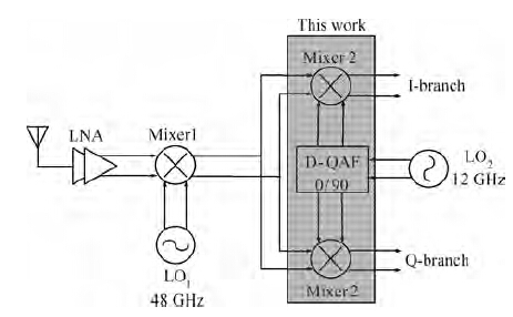
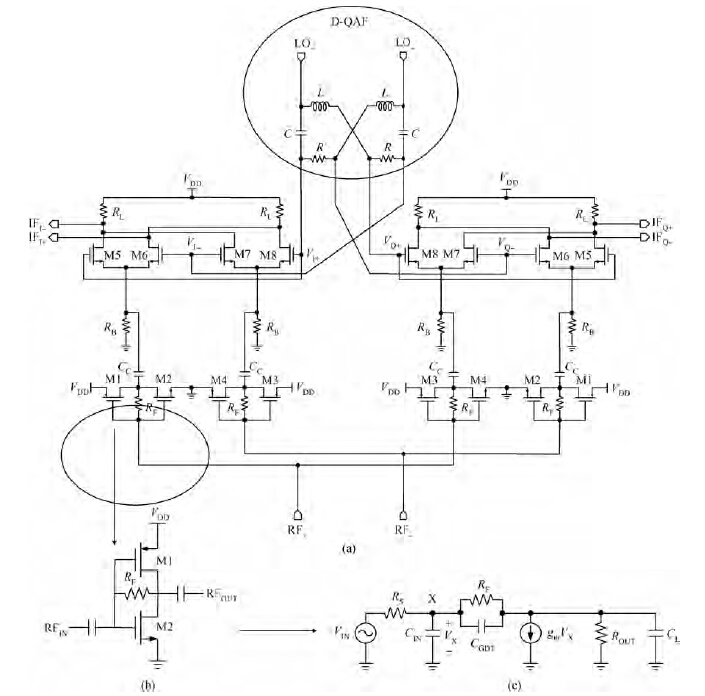
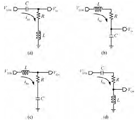
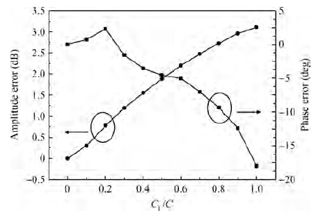
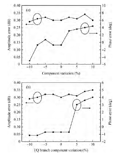
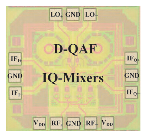
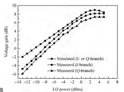
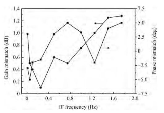
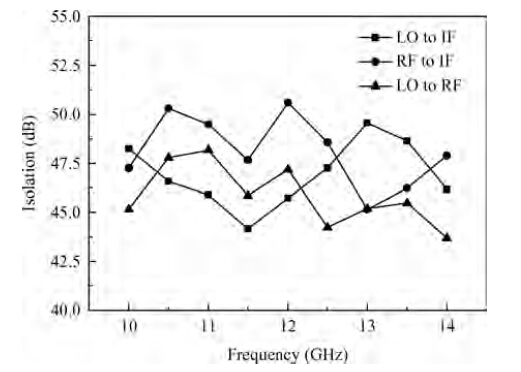
A down-conversion in-phase/quadrature (I/Q) mixer employing a folded-type topology, integrated with a passive differential quadrature all-pass filter (D-QAF), in order to realize the final down-conversion stage of a 60 GHz receiver architecture is presented in this work. Instead of employing conventional quadrature generation techniques such as a polyphase filter or a frequency divider for the local oscillator (LO) of the mixer, a passive D-QAF structure is employed. Fabricated in a 65 nm CMOS process, the mixer exhibits a voltage gain of 7-8 dB in an intermediate frequency (IF) band ranging from 10 MHz-1.75 GHz. A fixed LO frequency of 12 GHz is used to down-convert a radio frequency (RF) band of 10.25-13.75 GHz. The mixer displays a third order input referred intercept point (IIP3) ranging from -8.75 to -7.37 dBm for a fixed IF frequency of 10 MHz and a minimum single-sideband noise figure (SSB-NF) of 11.3 dB. The mixer draws a current of 6 mA from a 1.2 V supply voltage dissipating a power of 7.2 mW.


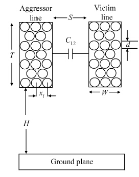
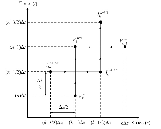
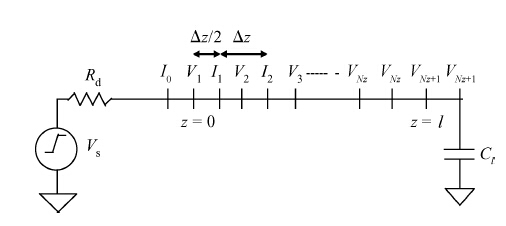
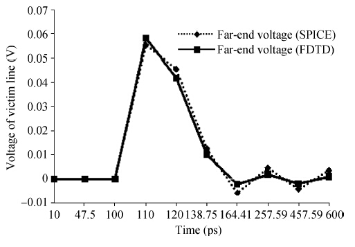
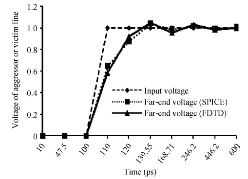
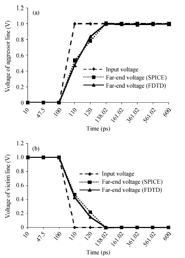
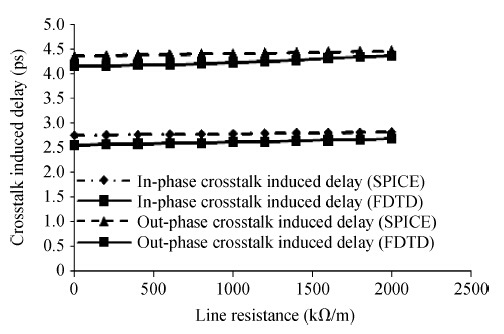
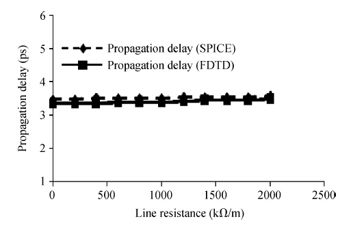
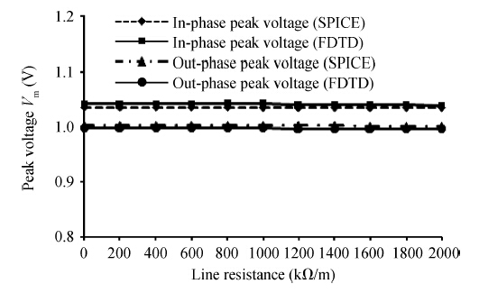
The equivalent electrical circuit model of a bundled single-walled carbon nanotube based distributed RLC interconnects is employed for the crosstalk analysis. The accurate time domain analysis and crosstalk effect in the VLSI interconnect has emerged as an essential design criteria. This paper presents a brief description of the numerical method based finite difference time domain (FDTD) technique that is intended for estimation of voltages and currents on coupled transmission lines. For the FDTD implementation, the stability of the proposed model is strictly restricted by the Courant condition. This method is used for the estimation of crosstalk induced propagation delay and peak voltage in lossy RLC interconnects. Both functional and dynamic crosstalk effects are analyzed in the coupled transmission line. The effect of line resistance on crosstalk induced delay, and peak voltage under dynamic and functional crosstalk is also evaluated. The FDTD analysis and the SPICE simulations are carried out at 32 nm technology node for the global interconnects. It is observed that the analytical results obtained using the FDTD technique are in good agreement with the SPICE simulation results. The crosstalk induced delay, propagation delay, and peak voltage obtained using the FDTD technique shows average errors of 4.9%, 3.4% and 0.46%, respectively, in comparison to SPICE.


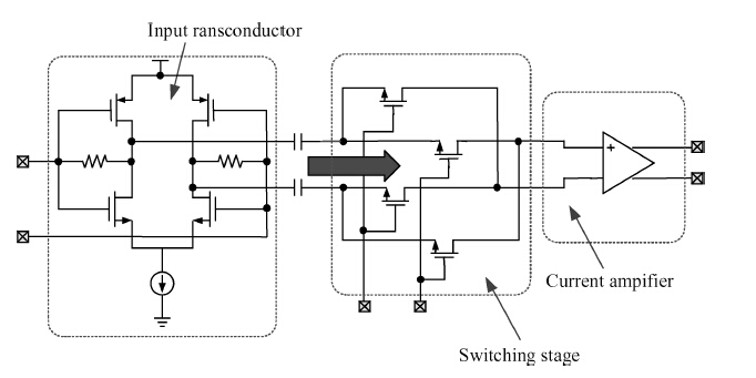
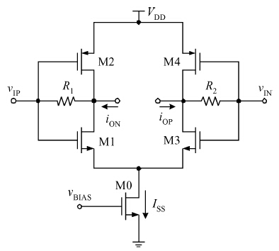
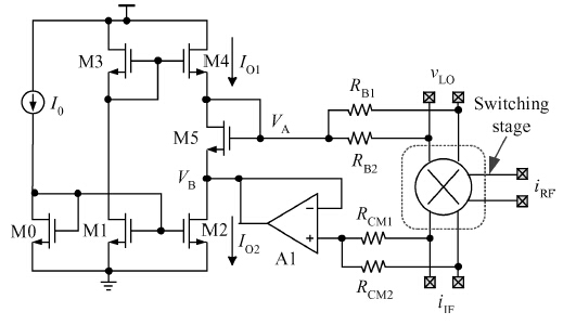
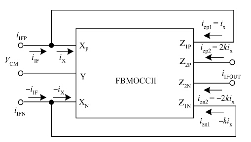
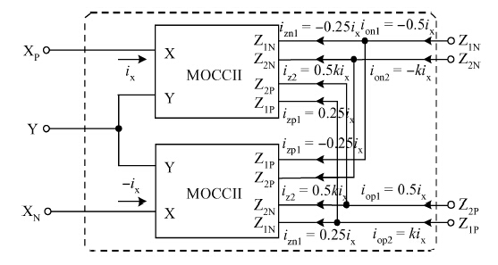
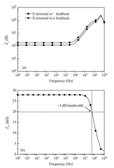
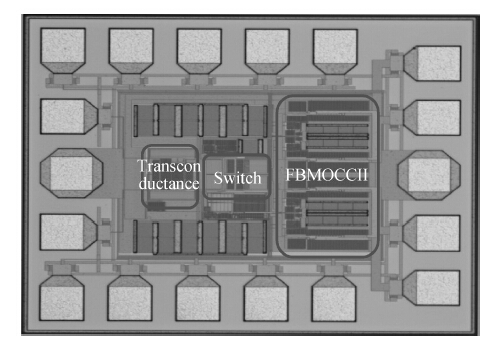
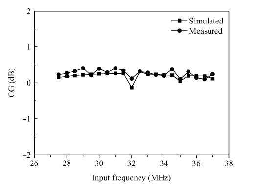
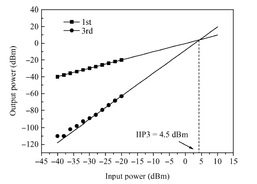
A passive current switch mixer was designed for the second IF down-conversion in a DRM/DAB receiver. The circuit consists of an input transconductance stage, a passive current switching stage, and a current amplifier stage. The input transconductance stage employs a self-biasing current reusing technique, with a resistor shunt feedback to increase the gain and output impedance. A dynamic bias technique is used in the switching stage to ensure the stability of the overdrive voltage versus the PVT variations. A current shunt feedback is introduced to the conventional low-voltage second-generation fully balanced multi-output current converter (FBMOCCII), which provides very low input impedance and high output impedance. With the circuit working in current mode, the linearity is effectively improved with low supply voltages. Especially, the transimpedance stage can be removed, which simplifies the design considerably. The design is verified with a SMIC 0.18 μ m RF CMOS process. The measurement results show that the voltage conversation gain is 1.407 dB, the NF is 16.22 dB, and the IIP3 is 4.5 dBm, respectively. The current consumption is 9.30 mA with a supply voltage of 1.8 V. This exhibits a good compromise among the gain, noise, and linearity for the second IF mixer in DRM/DAB receivers.


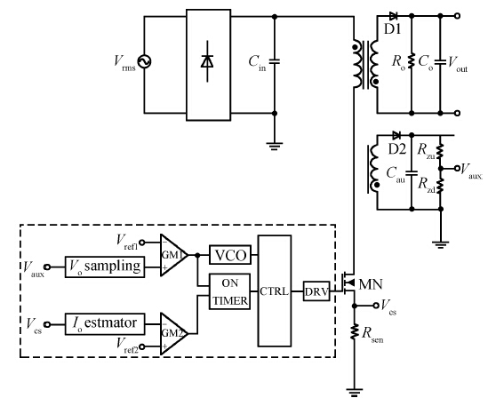
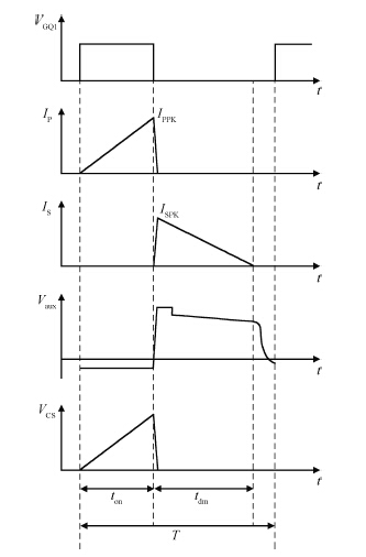
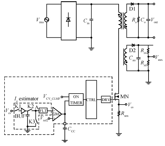
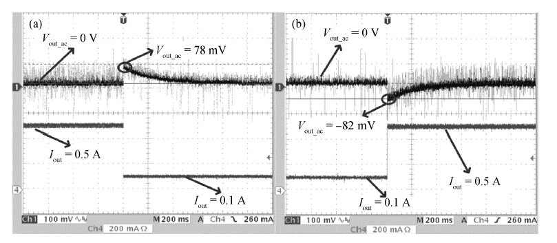
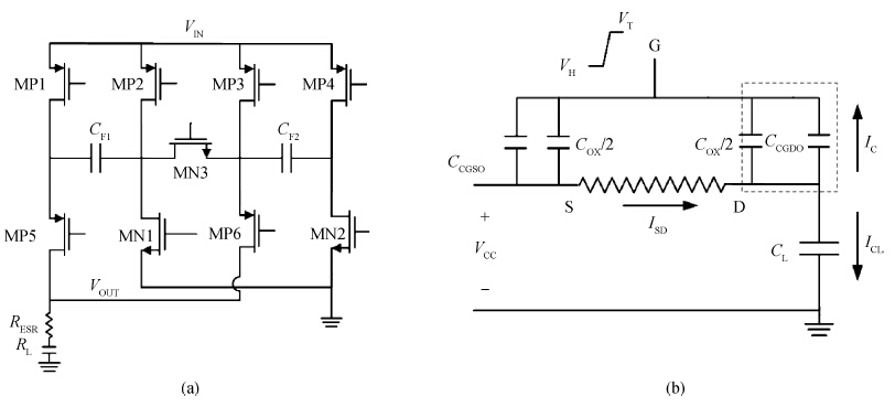
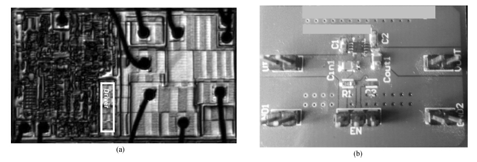
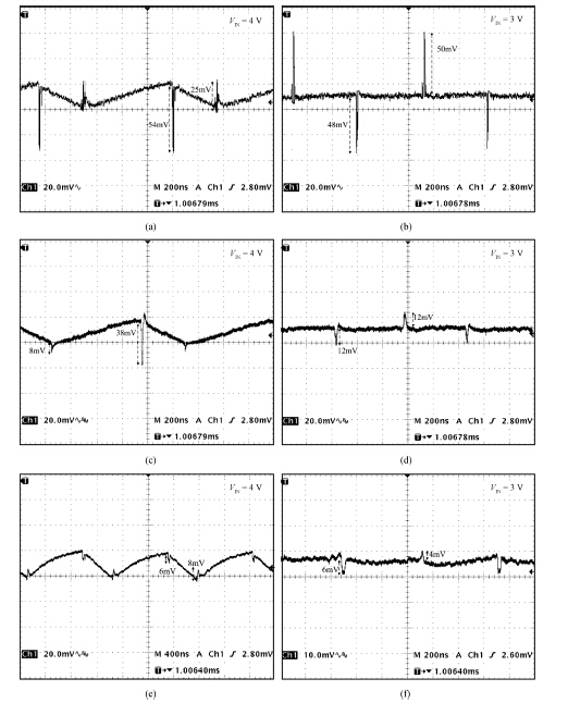
A 5.0-V 2.0-A flyback power supply controller providing constant-voltage (CV) and constant-current (CC) output regulation without the use of an optical coupler is presented. Dual-close-loop control is proposed here due to its better regulation performance of tolerance over process and temperature compared with open loop control used in common. At the same time, the two modes, CC and CV, could switch to each other automatically and smoothly according to the output voltage level not sacrificing the regulation accuracy at the switching phase, which overcomes the drawback of the digital control scheme depending on a hysteresis comparator to change the mode. On-chip compensation using active capacitor multiplier technique is applied to stabilize the voltage loop, eliminate an additional package pin, and save on the die area. The system consumes as little as 100 mW at no-load condition without degrading the transient response performance by utilizing the adaptive switching frequency control mode. The proposed controller has been implemented in a commercial 0.35-μ m 40-V BCD process, and the active chip area is 1.5 × 1.0 mm2. The total error of the output voltage due to line and load variations is less than ± 1.7%.


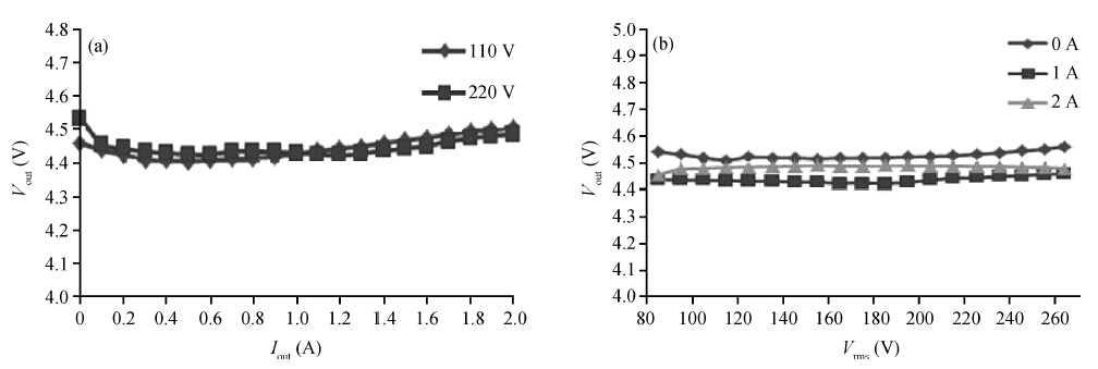

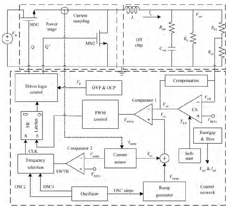
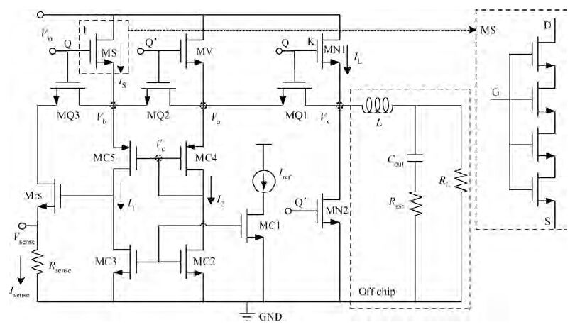
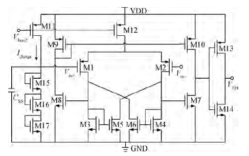
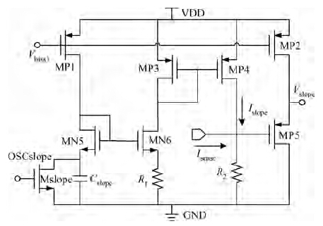
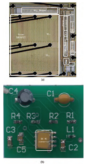
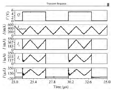
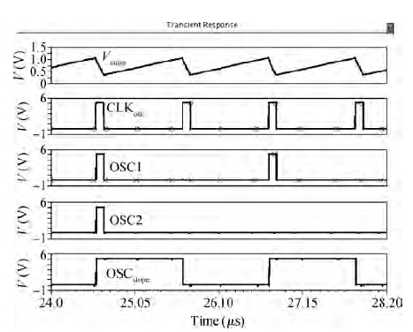
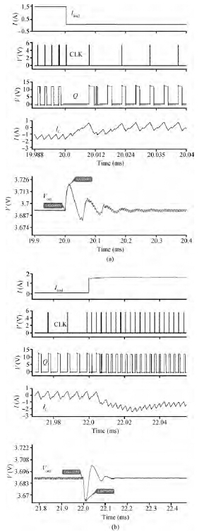
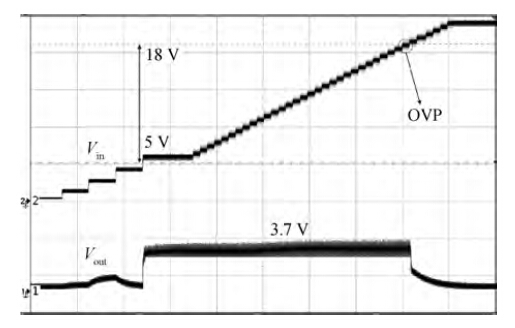
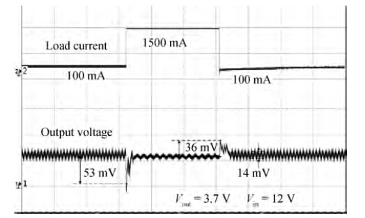
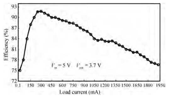
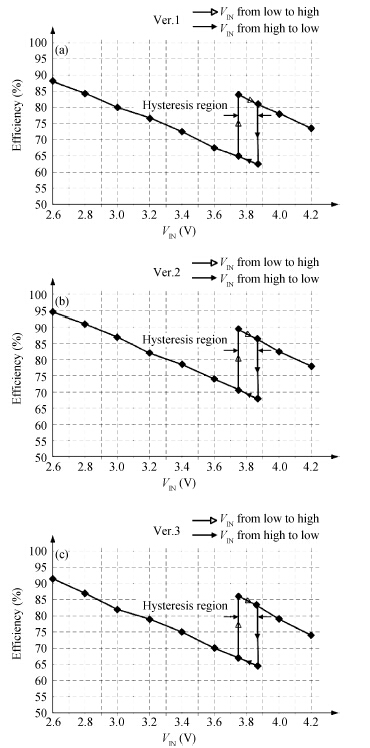
A current-mode PWM buck DC-DC converter is proposed. With the high-accuracy on-chip current sensor, the switching frequency can be selected automatically according to load requirements. This method improves efficiency and obtains an excellent transient response. The high accuracy of the current sensor is achieved by a simple switch technique without an amplifier. This has the direct benefit of reducing power dissipation and die size. Additionally, a novel soft-start circuit is presented to avoid the inrush current at the starting up state. Finally, this DC-DC converter is fabricated with the 0.5 μ m standard CMOS process. The chip occupies 3.38 mm2. The accuracy of the proposed current sensor can achieve 99.5% @ 200 mA. Experimental results show that the peak efficiency is 91.8%. The input voltage ranges from 5 to 18 V, while a 2 A load current can be obtained.


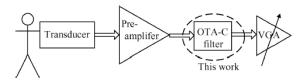
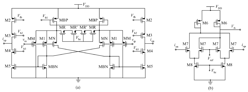
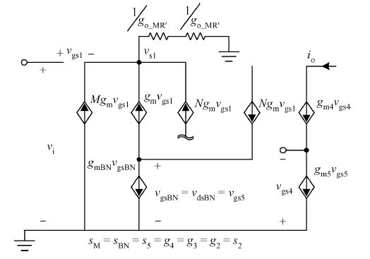
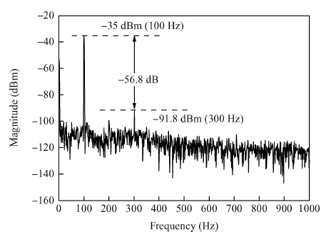
A fifth order operational transconductance amplifier-C (OTA-C) Butterworth type low-pass filter with highly linear range and less passband attenuation is presented for wearable bio-telemetry monitoring applications in a UWB wireless body area network. The source degeneration structure applied in typical small transconductance circuit is improved to provide a highly linear range for the OTA-C filter. Moreover, to reduce the passband attenuation of the filter, a cascode structure is employed as the output stage of the OTA. The OTA-based circuit is operated in weak inversion due to strict power limitation in the biomedical chip. The filter is fabricated in a SMIC 0.18-μ m CMOS process. The measured results for the filter have shown a passband gain of -6.2 dB, while the -3-dB frequency is around 276 Hz. For the 0.8 VPP sinusoidal input at 100 Hz, a total harmonic distortion (THD) of -56.8 dB is obtained. An electrocardiogram signal with noise interference is fed into this chip to validate the function of the designed filter.


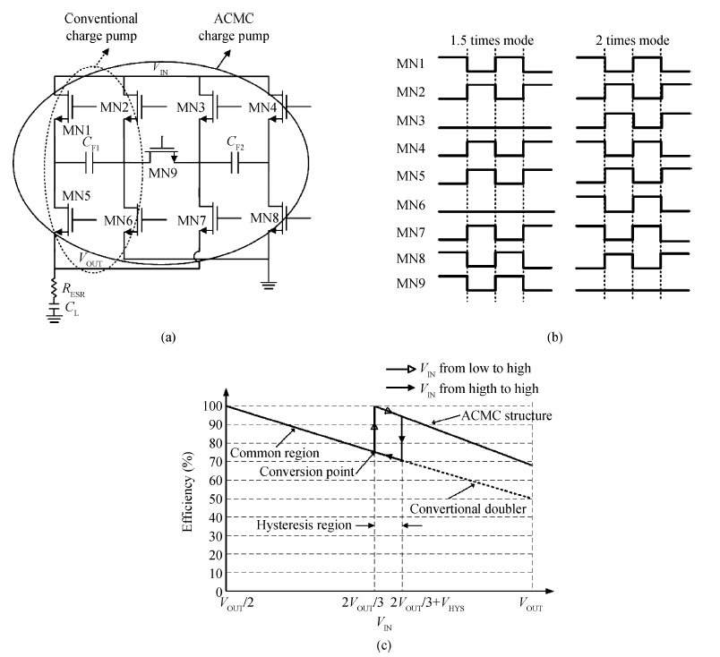
This paper presents an exact expression for switch-induced error voltage which would cause a spike voltage on the output capacitor of the automatic conversion mode change (ACMC) charge pumps. The spike voltage will introduce several undesired problems--large output voltage ripple, serious frequency noise and low efficiency. Some methods used for reducing the spike voltage are provided by the proposed expression. An equivalent lumped model is used for deducing the expression. The ACMC charge pump circuit has been designed in SILTERRA 0.18 μ m CMOS process. The experiment results show that the value of the spike voltage can match the expression well. Compared with three different improved versions, the spike voltage caused by the switch-induced error voltage can be reduced obviously.


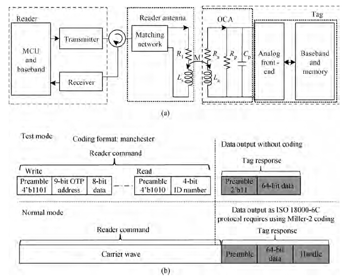
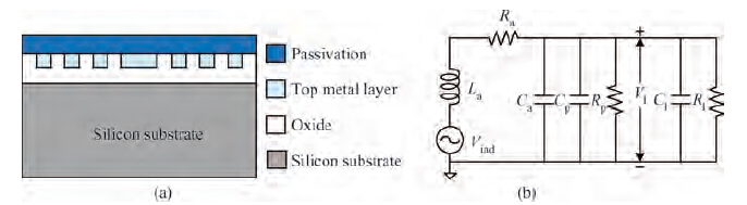
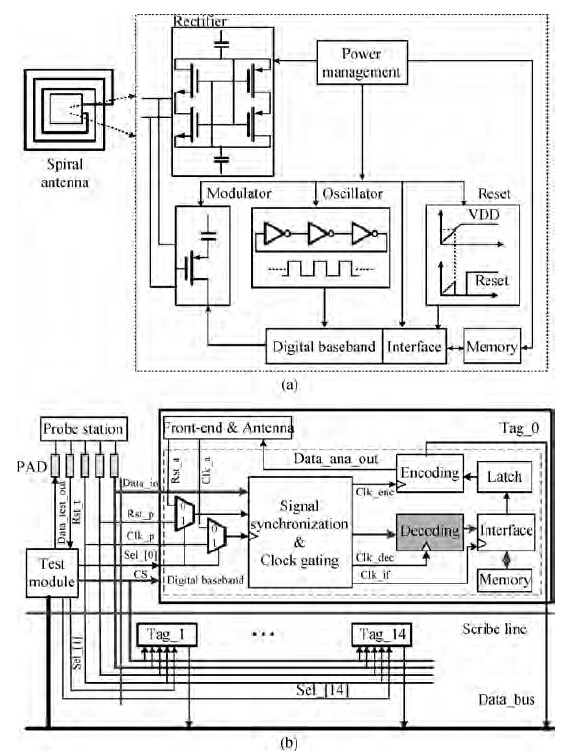
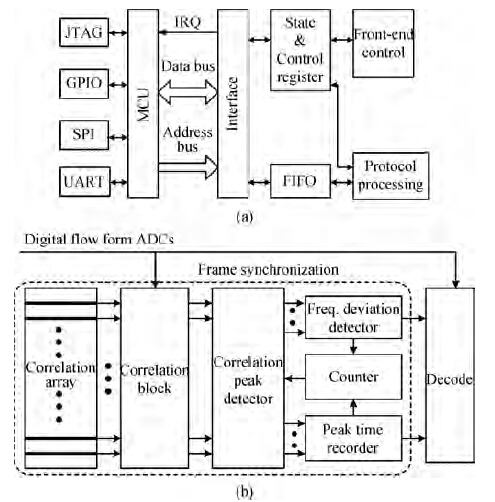
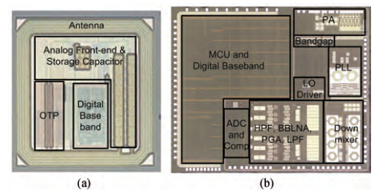
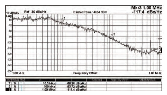
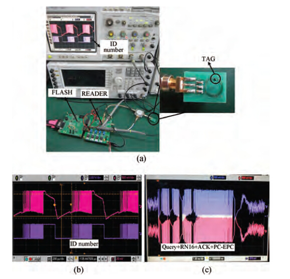
A UHF RF identification system based on the 0.18 μm CMOS process has been developed for short range and harsh size requirement applications, which is composed of a fully integrated tag and a special reader. The whole tag chip with the antenna takes up an area of 0.36 mm2, which is smaller than other reported tags with an on-chip antenna (OCA) using the standard CMOS process. A self-defined protocol is proposed to reduce the power consumption, and minimize the size of the tag. The specialized SOC reader system consists of the RF transceiver, digital baseband, MCU and host interface. Its power consumption is about 500 mW. Measurement results show that the system's reading range is 2 mm with 20 dBm reader output power. With an inductive antenna printed on a paper substrate around the OCA tag, the reading range can be extended from several centimeters to meters, depending on the shape and size of the inductive antenna.
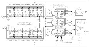
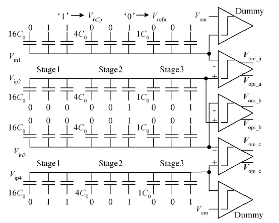
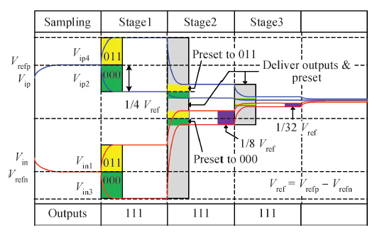
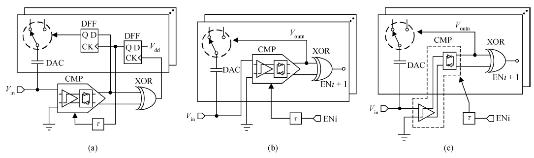
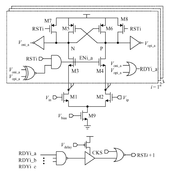
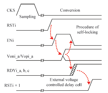
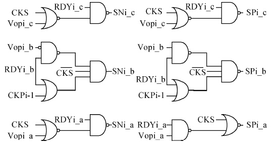
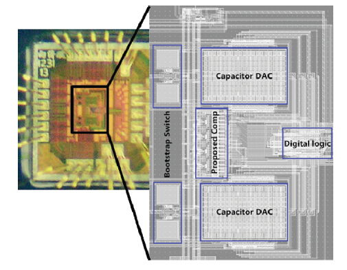
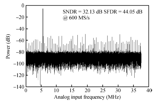
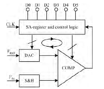
This paper presents a 6-b successive approximation register (SAR) ADC at the sampling rate of 600 MHz in a 65 nm CMOS process. To pursue high speed, this design employs the idea of the 2-b/stage. Based on this, the proposed structure with a new switching procedure is presented. Compared with traditional structures, it optimizes problems cause by mismatches of DACs and saves power. In addition, this paper takes advantage of distributed comparator topology to improve the speed, while the proposed structure and self-locking technique lighten the kickback and offset caused by multiple comparators. The measurement results demonstrate that the signal-to-noise plus distortion ratio (SNDR) is 32.13 dB and the spurious-free dynamic range (SFDR) is 44.05 dB at 600 MS/s with 5.6 MHz input. By contrast, the SNDR/SFDR respectively drops to 28.46/39.20 dB with Nyquist input. Fabricated in a TSMC 65 nm process, the SAR ADC core occupies an area of 0.045 mm2 and consumes power of 5.01 mW on a supply voltage of 1.2 V resulting in a figure of merit of 252 fJ/conversion-step.


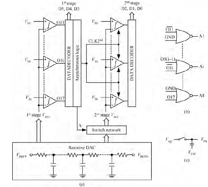
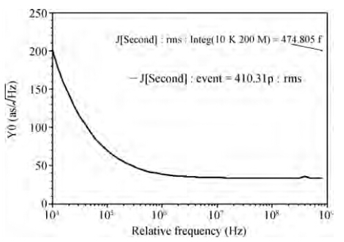
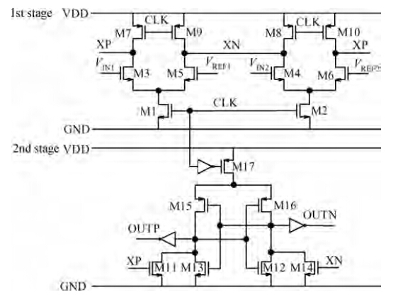
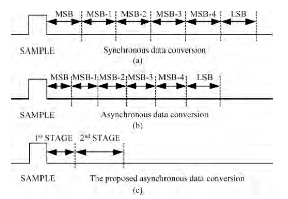
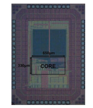
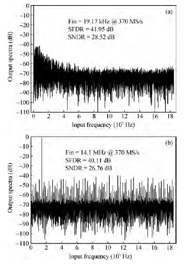
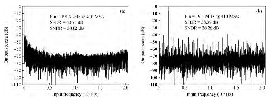
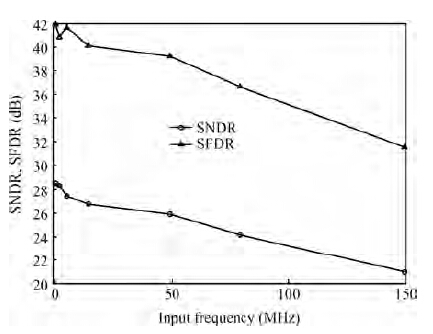
This paper presents a single channel, low power 6-bit 410-MS/s asynchronous successive approximation register analog-to-digital converter (SAR ADC) for ultrawide bandwidth (UWB) communication, prototyped in a SMIC 65-nm process. Based on the 3 bits/stage structure, resistive DAC, and the modified asynchronous successive approximation register control logic, the proposed ADC attains a peak spurious-free dynamic range (SFDR) of 41.95 dB, and a signal-to-noise and distortion ratio (SNDR) of 28.52 dB for 370 MS/s. At the sampling rate of 410 MS/s, this design still performs well with a 40.71-dB SFDR and 30.02-dB SNDR. A four-input dynamic comparator is designed so as to decrease the power consumption. The measurement results indicate that this SAR ADC consumes 2.03 mW, corresponding to a figure of merit of 189.17 fJ/step at 410 MS/s.


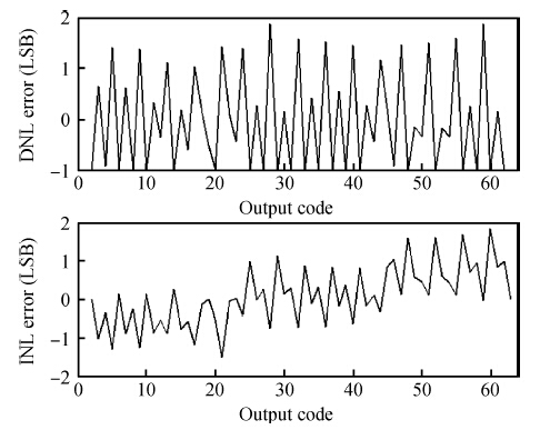
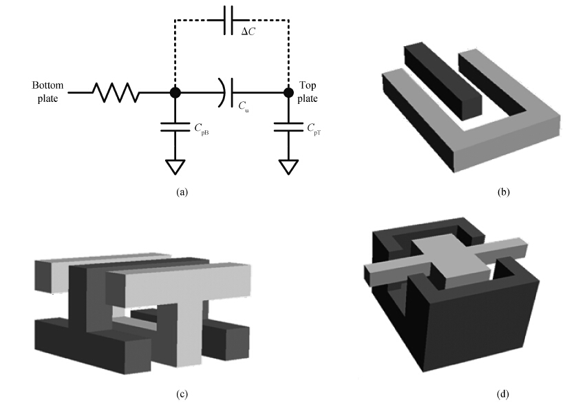
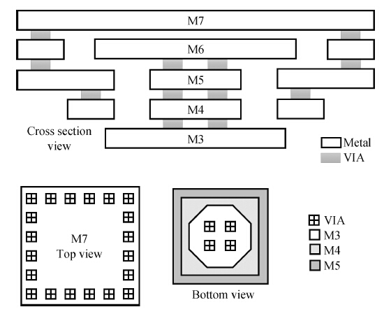
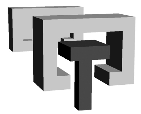
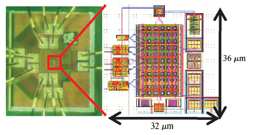
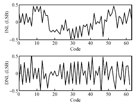
Asynchronous successive approximation register (SAR) analog-to-digital converters (ADC) feature high energy efficiency but medium performance. From the point of view of speed, the key bottleneck is the unit capacitor size. In this paper, a small size three-dimensional (3-D) metal-oxide-metal (MOM) capacitor is proposed. The unit capacitor has a capacitance of 1-fF. It shapes as an umbrella, which is designed for fast settling consideration. A comparison among the proposed capacitor with other 3-D MOM capacitors is also given in the paper. To demonstrate the effectiveness of the MOM capacitor, a 6-b capacitive DAC is implemented in TSMC 1P9M 65 nm LP CMOS technology. The DAC consumes a power dissipation of 0.16 mW at the rate of 100 MS/s, excluding a source-follower based output buffer. Static measurement result shows that INL is less than ± 1 LSB and DNL is less than ± 0.5 LSB. In addition, a 100 MS/s 9-bit SAR ADC with the proposed 3-D capacitor is simulated.

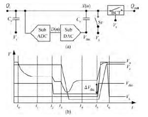
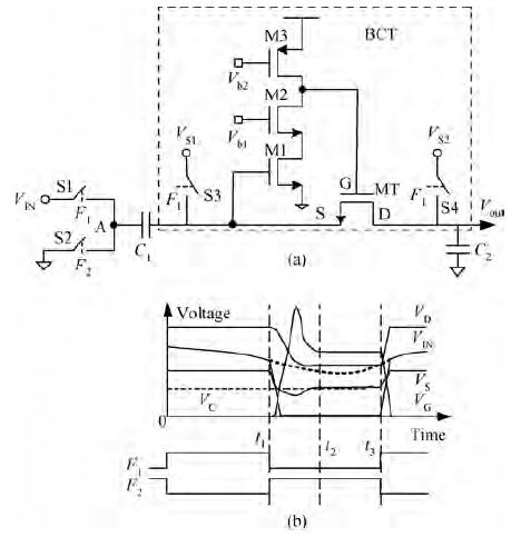
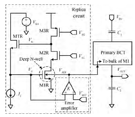
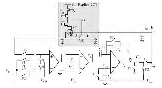
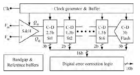
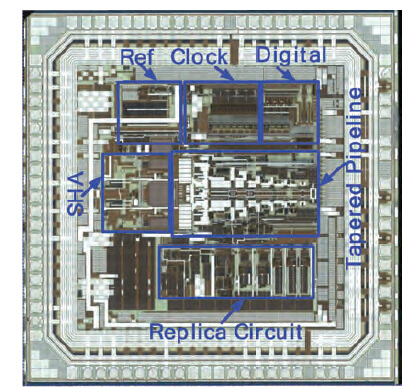
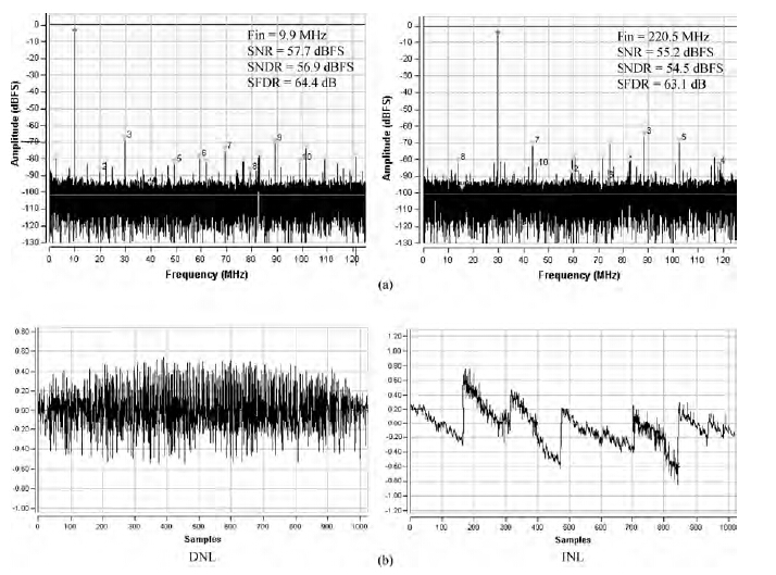
A low power 10-bit 250 MSPS charge-domain (CD) pipelined analog-to-digital converter (ADC) is introduced. The ADC is implemented in MOS bucket-brigade devices (BBDs) based CD pipelined architecture. A replica controlled boosted charge transfer (BCT) circuit is introduced to reject the influence of PVT variations on the charge transfer process. Based on replica controlled BCT, the CD pipelined ADC is designed and realized in a 1P6M 0.18 μ m CMOS process. The ADC achieves the SFDR of 64.4 dB, the SNDR of 56.9 dBFS and the ENOB of 9.2 for a 9.9 MHz input; and the SFDR of 63.1 dB, the SNR of 55.2 dBFS, the SNDR of 54.5 dBFS and the ENOB of 8.7 for a 220.5 MHz input at full sampling rate. The DNL is +0.5/-0.55 LSB and INL is +0.8/-0.85 LSB. The power consumption of the prototype ADC is only 45 mW at 1.8 V supply and it occupies an active die area of 1.56 mm2.


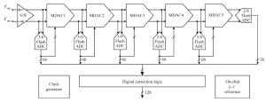
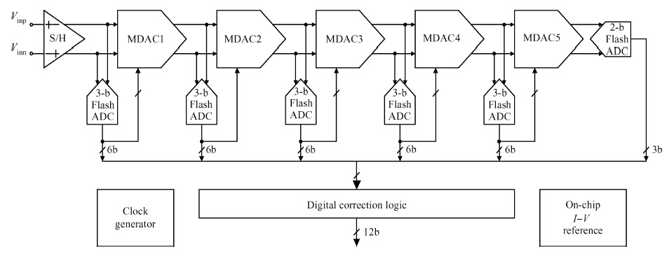
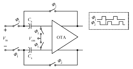
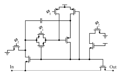
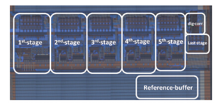
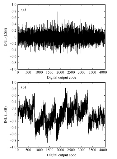
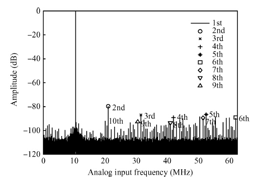
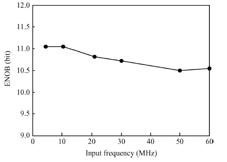
This paper describes a 12-bit 125-MS/s pipelined analog-to-digital converter (ADC) that is implemented in a 0.18 μ m CMOS process. A gate-bootstrapping switch is used as the bottom-sampling switch in the first stage to enhance the sampling linearity. The measured differential and integral nonlinearities of the prototype are less than 0.79 least significant bit (LSB) and 0.86 LSB, respectively, at the full sampling rate. The ADC exhibits an effective number of bits (ENOB) of more than 11.05 bits at the input frequency of 10.5 MHz. The ADC also achieves a 10.5 bits ENOB with the Nyquist input frequency at the full sample rate. In addition, the ADC consumes 62 mW from a 1.9 V power supply and occupies 1.17 mm2, which includes an on-chip reference buffer. The figure-of-merit of this ADC is 0.23 pJ/step.


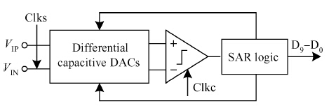
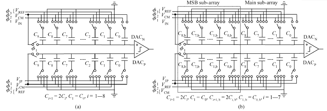
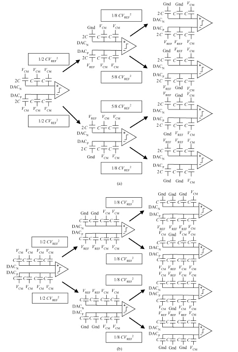
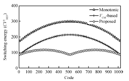
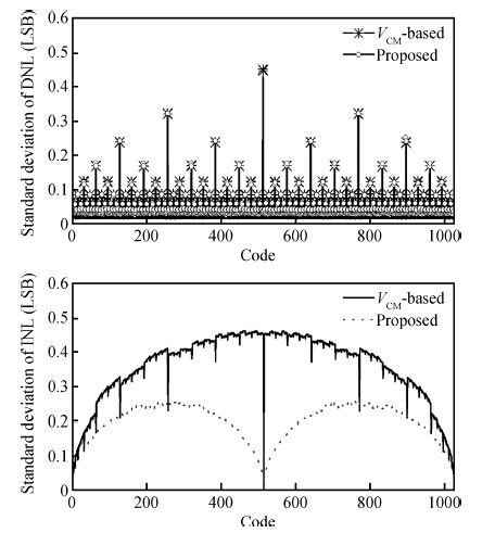
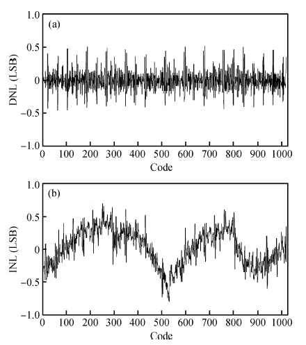
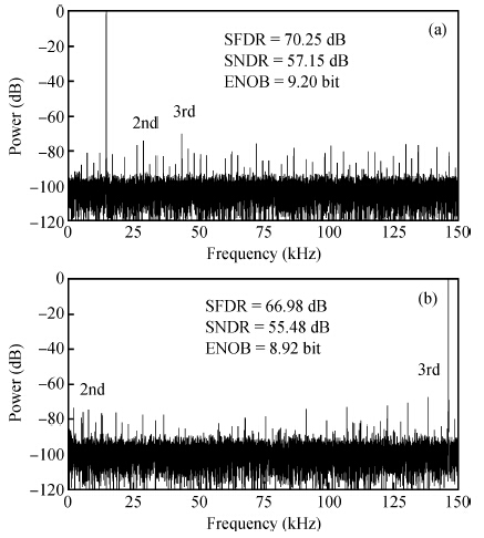
An energy-efficient and highly linear capacitor switching procedure for successive approximation register (SAR) ADCs is presented. The proposed switching procedure achieves 37% less switching energy when compared to the well-known VCM-based switching scheme. Moreover, the proposed method shows better linearity than the VCM-based one. The proposed switching procedure is applied to a 10-bit 1.0 V 300 kS/s SAR ADC implemented in 0.18 μ m standard CMOS. The measured results show the SAR ADC achieves an SNDR of 55.48 dB, SFDR of 66.98 dB, and consumes 2.13 μ W at a 1.0 V power supply, resulting in a figure-of-merit of 14.66 fJ/conversion-step. The measured peak DNL and INL are 0.52/-0.47 LSB and 0.72/-0.79 LSB, respectively, and the peak INL is observed at 1/4(VFS) and 3/4(VFS), the same as the static nonlinearity model.