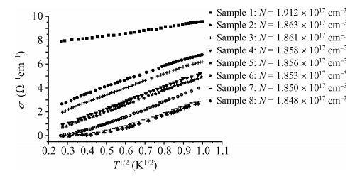
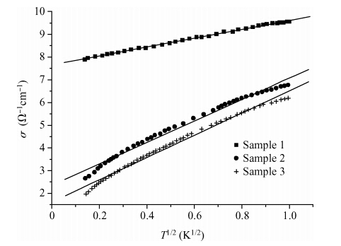
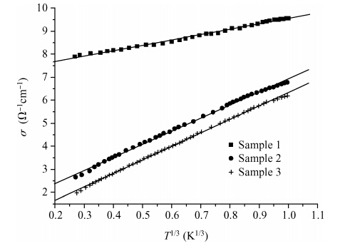
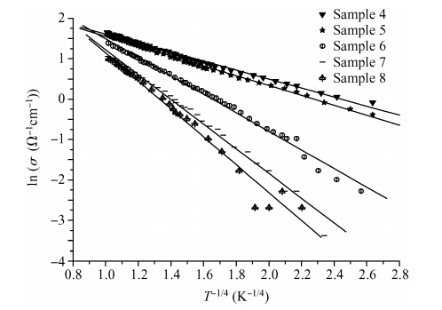
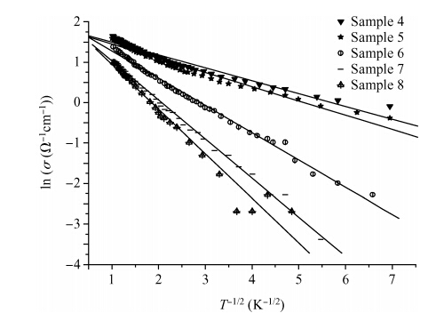
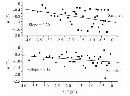
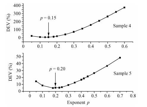
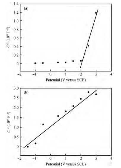
The results of the metal-insulator transition (MIT) induced by impurity concentration are presented in the case of metallic and insulating samples 70Ge:Ga p-type. The eight samples studied have Ga concentrations N ranging from 1.848 × 10¹⁷ to 1.912 × 1017cm-3. The conductivity measurements were carried out at low temperature in the range 1 to 0.019 K. We provide physical explanations to explain the behaviors of the temperature dependence of the electrical conductivity in both sides of the MIT. The data are for a 70Ge:Ga sample prepared and reported by Itoh et al. in Ref. [Itoh K M, Watanabe M, Ootuka Y, et al. J Phys Soc Jpn, 2004, 73(1): 173].
Issue Browser
Volume 36, Issue 6,
Jun 2015


J. Semicond.
2015, 36(6): 062002 doi: 10.1088/1674-4926/36/6/062002

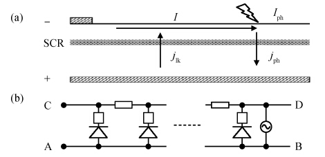
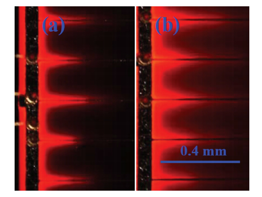
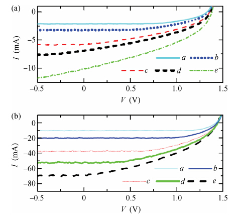
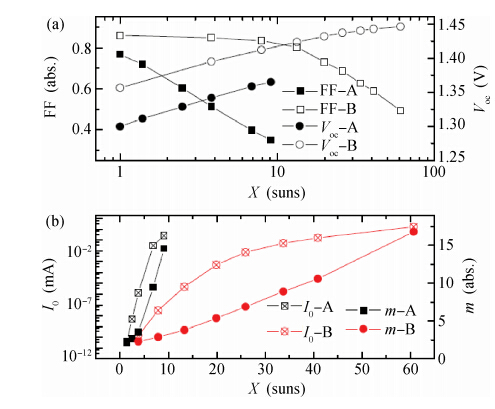
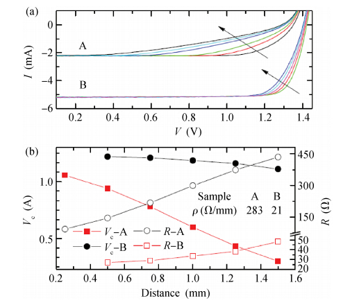
An alternative way is proposed to interpret I-V characteristics of GaInP single-junction solar cells by position-dependent leakage of photocurrent. With this approach, the I-V curves of solar cells under non-uniform illumination are well analyzed. The effective spreading resistance is also extracted to understand the dynamic behavior of between the open-circuit voltage and short-circuit current points. The conditions under which the one-diode model will fail are addressed in detail. These analyses are also applicable for a characterization of the I-V curves with lateral voltage distribution under uniform illumination.


J. Semicond.
2015, 36(6): 063001 doi: 10.1088/1674-4926/36/6/063001

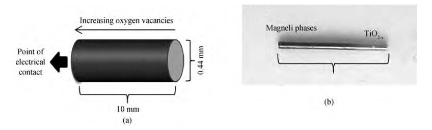
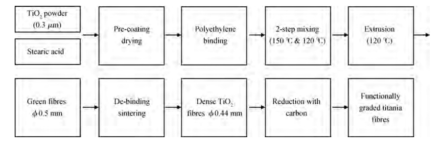
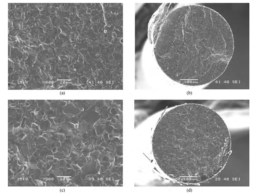
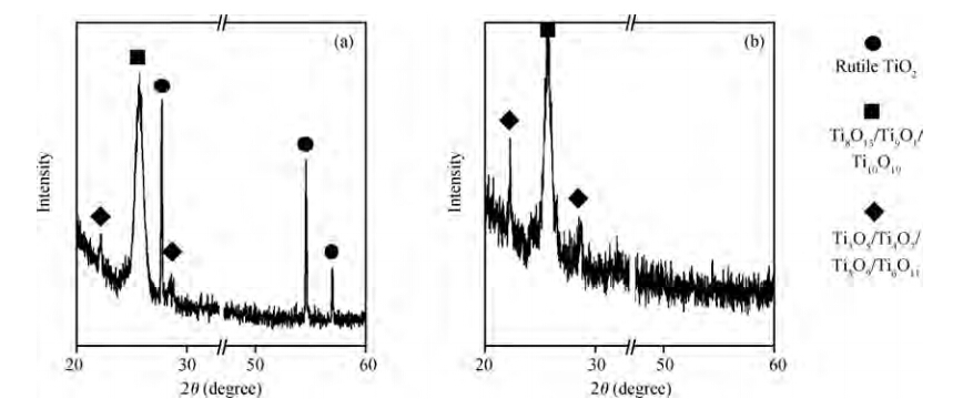
The photo-electro-chemical (PEC) splitting of water requires semiconductor materials with a minimum energy gap of 1.23 eV along with conduction and valence bands overlapping the oxidation of H2O and reduction of H+ respectively. The aim of this work is to overcome the limitations of stoichiometric titania by manufacturing fine scale fibres that exhibit a compositional gradient of oxygen vacancies across the fibre length. In such a fibre configuration the fibre end that is chemically reduced to a relatively small extent performs as the photoanode and the oxygen vacancies enhance the absorption of light. The fibre end that is reduced the most consists of Magnéli phases and exhibits metallic electrical conductivity that enhances the electron-hole separation. The structure and composition of the functionally graded fibres, which were manufactured through extrusion, pressureless sintering and carbo-thermal reduction, are studied using XRD and electron microscopy. Electrochemical impedance spectroscopy measurements were performed in a three-electrode electrochemical system and showed that the oxygen vacancies in the functionally graded fibres affect the flat band potential and have increased carrier density. The efficiency of the system was evaluated with PEC measurements that shows higher efficiency for the functionally graded fibres compared to homogeneous TiO2 or Magnéli phase fibres. The functionally graded and fine scale fibres have the potential to be used as an array of active fibres for water splitting applications.


J. Semicond.
2015, 36(6): 063002 doi: 10.1088/1674-4926/36/6/063002

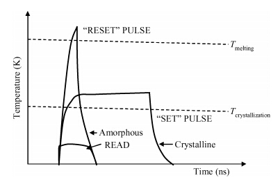
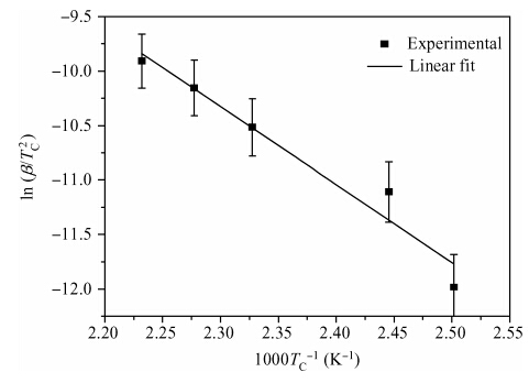
The crystallization kinetics of Sn40Se60 thin films has been successfully investigated using sheet resistance versus temperature measurements. Thermal evaporation was used to deposit the films on ordinary glass substrates. The crystallization temperature for Sn40Se60 thin film was found to be 156.6 ± 0.3 ℃. In the as-deposited state, the sheet resistance was found to be 195 MΩ, this value declined to 1560 Ω/口 upon annealing. The value of activation energy obtained from the Kissinger plot was 0.62 ± 0.07 eV. From the results obtained, Sn40Se60 is a promising alloy for PCM application because of its high electrical contrast, high crystallization temperature, and relatively high activation energy.

J. Semicond.
2015, 36(6): 063003 doi: 10.1088/1674-4926/36/6/063003

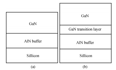
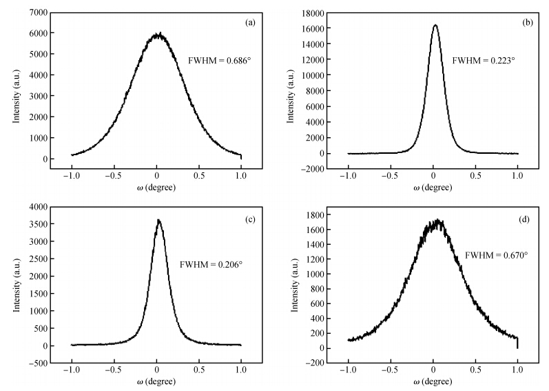
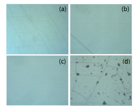
A method for growing GaN epitaxial layer on Si (111) substrate is investigated. Due to the large lattice mismatch between GaN and AlN, GaN grown directly above an AlN buffer layer on the Si substrate turns out to be of poor quality. In this study, a GaN transition layer is grown additionally on the AlN buffer before the GaN epitaxial growth. By changing the growth conditions of the GaN transition layer, we can control the growth and merging of islands and control the transfer time from 3D to 2D growth mode. With this method, the crystalline quality of the GaN epitaxial layer can be improved and the crack density is reduced. Here, we have investigated the impact of a transition layer on the crystalline quality and stress evolution of a GaN epitaxial layer with methods of X-ray diffraction, optical microscopy and in situ reflectivity trace. With the increasing thickness of transition layer, the crack decreases and the crystalline quality is improved. But when the transition layer exceeds a critical thickness, the crystalline quality of the epilayer becomes lower and the crack density increases.

J. Semicond.
2015, 36(6): 063004 doi: 10.1088/1674-4926/36/6/063004

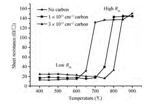
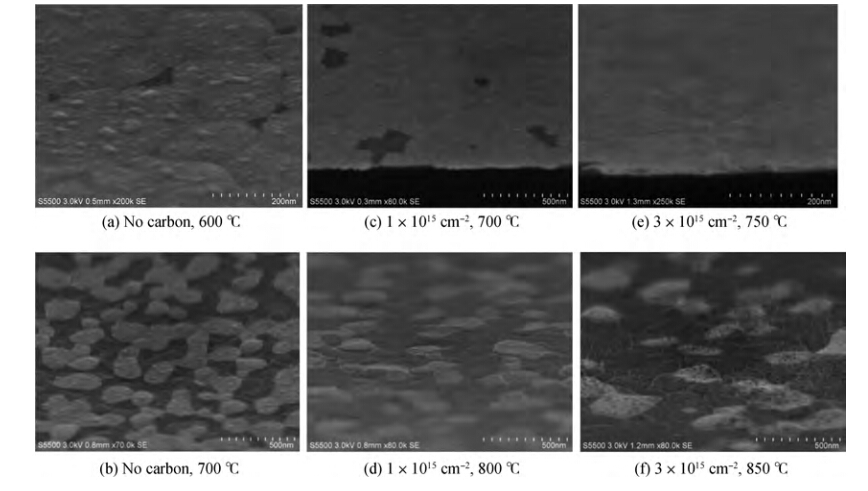
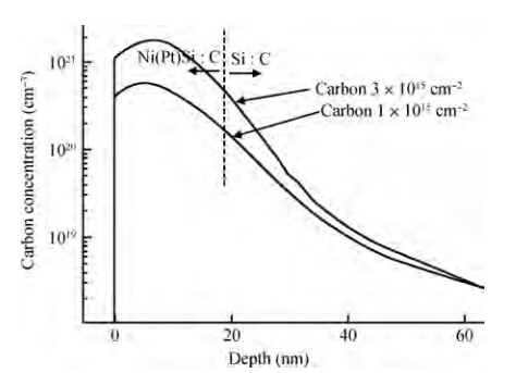
The effects of a carbon implant on thermal stability of Ni0.95(Pt0.05)Si films are investigated by implanting carbon of different doses into Si substrates before silicidation with two steps of rapid thermal annealing. Compared with the Ni0.95(Pt0.05)Si films without carbon implanting, the thermal stability of Ni0.95(Pt0.05)Si films with two carbon implant doses are improved 100 ℃ (1 × 1015cm-2) and 150 ℃ (3 × 1015cm-2

J. Semicond.
2015, 36(6): 063005 doi: 10.1088/1674-4926/36/6/063005

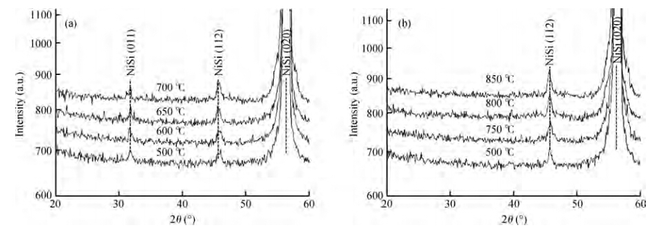
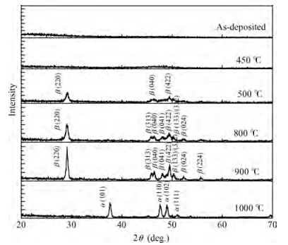
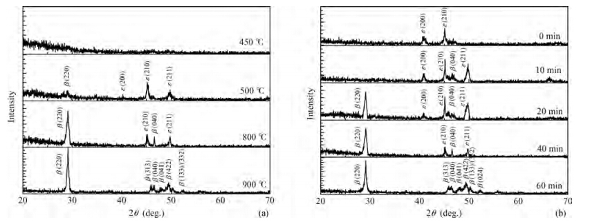
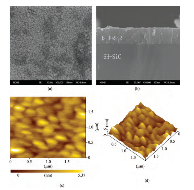
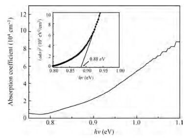
β-FeSi2 thin films have been successfully prepared by magnetron sputtering and post rapid thermal annealing method on 6H-SiC (0001) substrates using a FeSi2 target and a Si target. X-ray diffraction (XRD) and Raman spectroscopy are applied to analyze the formation of β-FeSi2 films. XRD spectra reveal that the amorphous FeSi2 films are transformed to β-FeSi2 phase as the annealing temperature is increased from 500 to 900 ℃ for 5 min and the optimal annealing temperature is 900 ℃. The formation of β-FeSi2 is also confirmed by Raman spectroscopy. Scanning electron microscope (SEM) observations indicate that the film is flat, relatively compact and the interface between β-FeSi2 and 6H-SiC is clear. Atomic force microscope (AFM) measurements demonstrate that the surface roughness confirmed by the root mean square (RMS) of the β-FeSi2 film is 0.87 nm. Near-infrared spectrophotometer observation shows that the absorption coefficient is of the order of 105cm-1 and the optical band-gap of the β-FeSi2 film is 0.88 eV. The β-FeSi2 film with high crystal quality is fabricated by co-sputtering a FeSi2 target and a Si target for 60 min and annealing at 900 ℃ for 5 min.


J. Semicond.
2015, 36(6): 064001 doi: 10.1088/1674-4926/36/6/064001

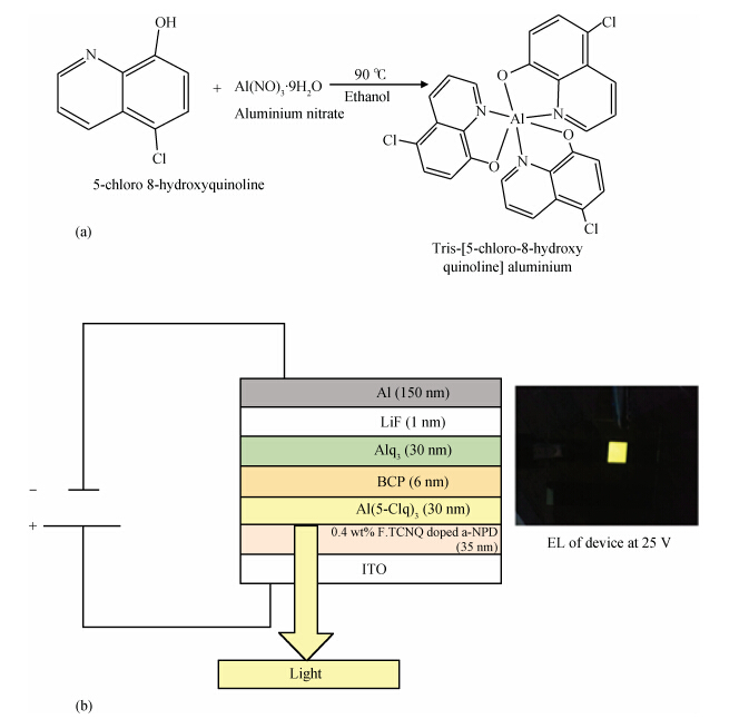
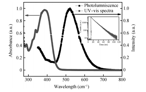
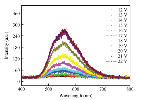
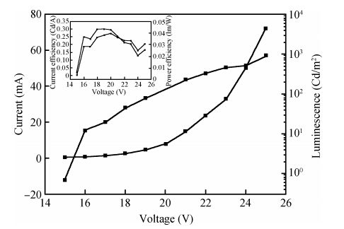
A new electroluminescent material tris-[5-choloro-8-hydroxyquinoline] aluminum has been synthesized and characterized. Solution of this material Al(5-Clq)3 in toluene showed absorption maxima at 385 nm which was attributed to the moderate energy (π-π*) transitions of the aromatic rings. The photoluminescence spectrum of Al(5-Clq)3 in toluene solution showed a peak at 522 nm. This material shows thermal stability up to 400 ℃. The structure of the device is ITO/0.4 wt%F4-TCNQ doped α-NPD (35 nm) / Al(5-Clq)3(30 nm)/ BCP (6 nm)/ Alq3(30 nm)/ LiF (1 nm)/Al(150 nm). This device exhibited a luminescence peak at 585 nm (CIE coordinates, x= 0.39, y= 0.50). The maximum luminescence of the device was 920 Cd/m2 at 25 V. The maximum current efficiency of OLED was 0.27 Cd/A at 20 V and maximum power efficiency was 0.04 lm/W at 18 V.
J. Semicond.
2015, 36(6): 064002 doi: 10.1088/1674-4926/36/6/064002

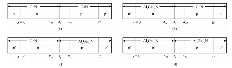
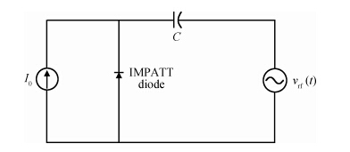
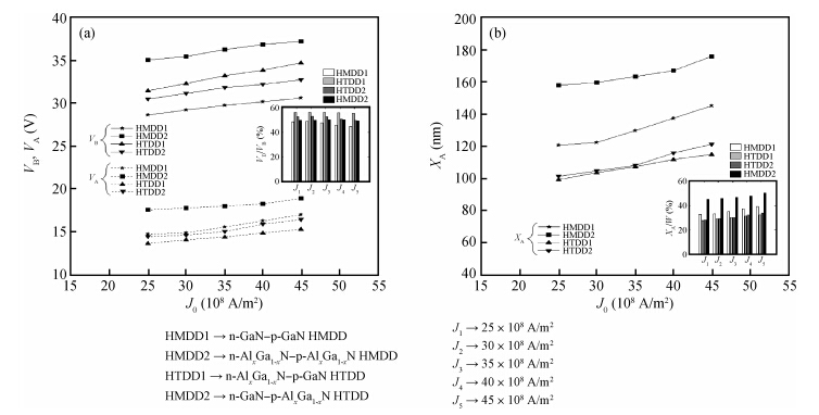
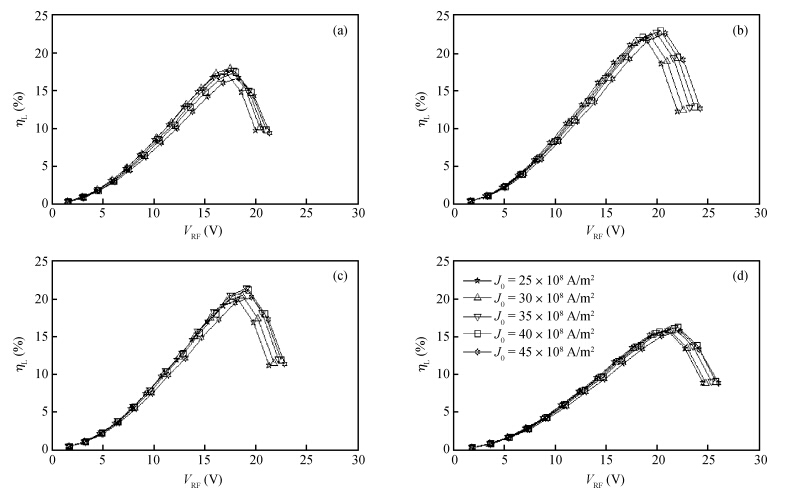
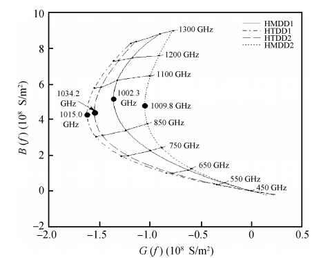
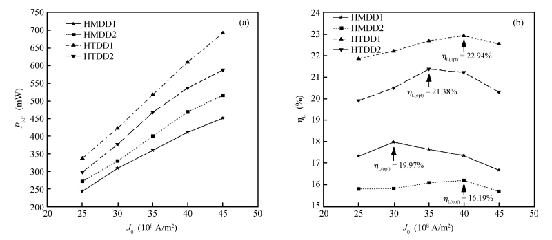
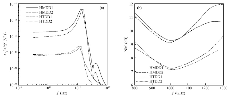
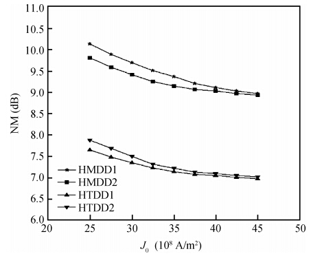
Simulation studies are made on the large-signal RF performance and avalanche noise properties of heterojunction double-drift region (DDR) impact avalanche transit time (IMPATT) diodes based on AlxGa1-xN/GaN material system designed to operate at 1.0 THz frequency. Two different heterojunction DDR structures such as n-Al0.4Ga0.6N/p-GaN and n-GaN/p-Al0.4Ga0.6N are proposed in this study. The large-signal output power, conversion efficiency and noise properties of the heterojunction DDR IMPATTs are compared with homojunction DDR IMPATT devices based on GaN and Al0.4Ga0.6N. The results show that the n-Al0.4Ga0.6N/p-GaN heterojunction DDR device not only surpasses the n-GaN/p-Al0.4Ga0.6N DDR device but also homojunction DDR IMPATTs based on GaN and Al0.4Ga0.6N as regards large-signal conversion efficiency, power output and avalanche noise performance at 1.0 THz.

J. Semicond.
2015, 36(6): 064003 doi: 10.1088/1674-4926/36/6/064003

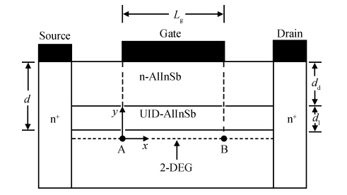
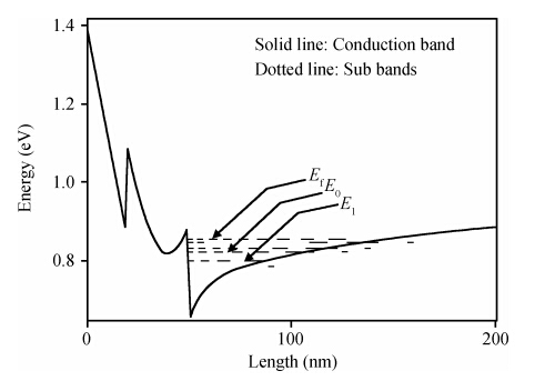
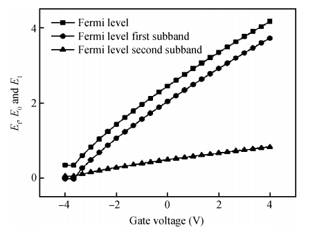
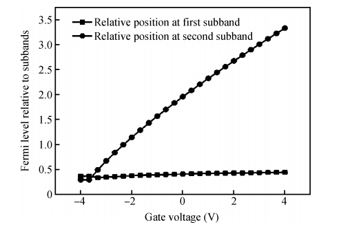
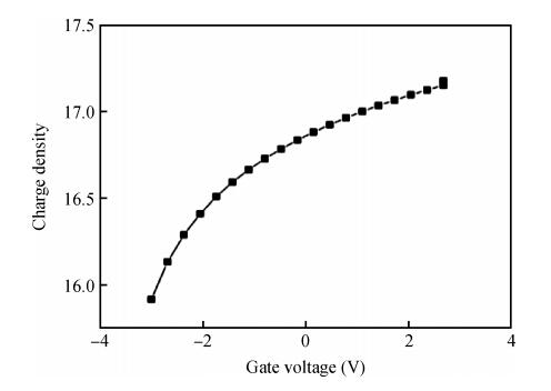
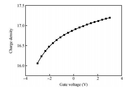
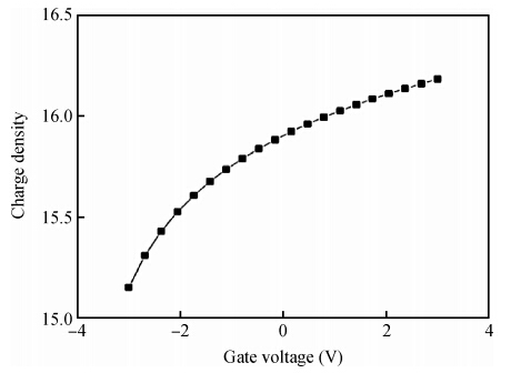
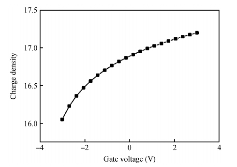
A compact model is proposed to derive the charge density of the AlInSb/InSb HEMT devices by considering the variation of Fermi level, the first subband, the second subband and sheet carrier charge density with applied gate voltage. The proposed model considers the Fermi level dependence of charge density and vice versa. The analytical results generated by the proposed model are compared and they agree well with the experimental results. The developed model can be used to implement a physics based compact model for an InSb HEMT device in SPICE applications.


J. Semicond.
2015, 36(6): 064004 doi: 10.1088/1674-4926/36/6/064004

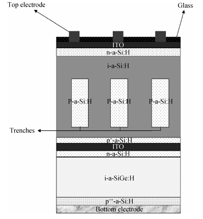
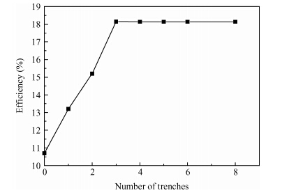
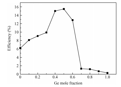
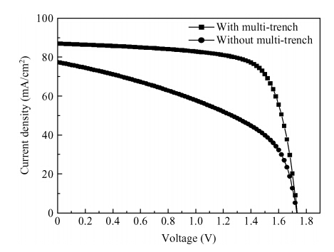
We present a new approach based on the multi-trench technique to improve the electrical performances, which are the fill factor and the electrical efficiency. The key idea behind this approach is to introduce a new multi-trench region in the intrinsic layer, in order to modulate the total resistance of the solar cell. Based on 2-D numerical investigation and optimization of amorphous SiGe double-junction (a-Si:H/a-SiGe:H) thin film solar cells, in the present paper numerical models of electrical and optical parameters are developed to explain the impact of the multi-trench technique on the improvement of the double-junction solar cell electrical behavior for high performance photovoltaic applications. In this context, electrical characteristics of the proposed design are analyzed and compared with conventional amorphous silicon double-junction thin-film solar cells.


J. Semicond.
2015, 36(6): 064005 doi: 10.1088/1674-4926/36/6/064005

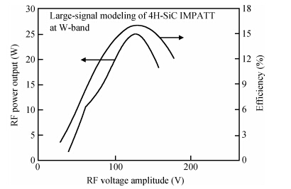
A full-scale, self-consistent, non-linear, large-signal model of double-drift hetero-structure IMPATT diode with general doping profile is derived. This newly developed model, for the first time, has been used to analyze the large-signal characteristics of hexagonal SiC-based double-drift IMPATT diode. Considering the fabrication feasibility, the authors have studied the large-signal characteristics of Si/SiC-based hetero-structure devices. Under small-voltage modulation (~ 2%, i.e. small-signal conditions) results are in good agreement with calculations done using a linearised small-signal model. The large-signal values of the diode's negative conductance (5 × 10⁶S/m2), susceptance (10.4 × 10⁷ S/m2}), average breakdown voltage (207.6 V), and power generating efficiency (15%, RF power: 25.0 W at 94 GHz) are obtained as a function of oscillation amplitude (50% of DC breakdown voltage) for a fixed average current density. The large-signal calculations exhibit power and efficiency saturation for large-signal (> 50%) voltage modulation and thereafter decrease gradually with further increasing voltage-modulation. This generalized large-signal formulation is applicable for all types of IMPATT structures with distributed and narrow avalanche zones. The simulator is made more realistic by incorporating the space-charge effects, realistic field and temperature dependent material parameters in Si and SiC. The electric field snap-shots and the large-signal impedance and admittance of the diode with current excitation are expressed in closed loop form. This study will act as a guide for researchers to fabricate a high-power Si/SiC-based IMPATT for possible application in high-power MM-wave communication systems.

J. Semicond.
2015, 36(6): 064006 doi: 10.1088/1674-4926/36/6/064006

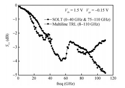
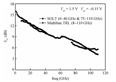
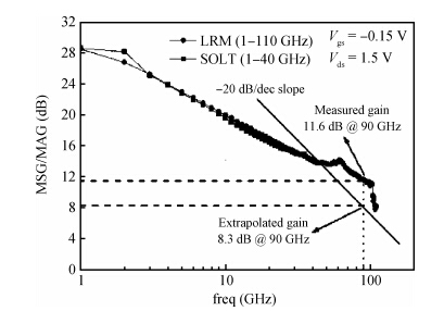
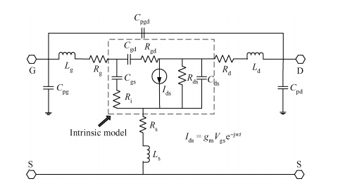
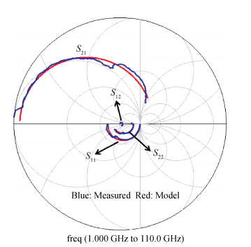
A quantitative comparison of multiline TRL (thru-reflect-line) and LRM (line-reflect-match) on-wafer calibrations for scattering parameters (S-parameters) measurement of InP-based PHEMTs is presented. The comparison is undertaken for the first time and covers a frequency range from 70 kHz to 110 GHz. It is demonstrated that the accuracy of multiline TRL and LRM calibration is in good agreement. Both methods outperform the conventional SOLT calibration in the full frequency band up to 110 GHz. Then the excellent RF performance is obtained by extrapolation on the basis of inflection point, including a maximum current gain cut-off frequency ft of 247 GHz and a maximum oscillation frequency fmax of 392 GHz. The small-signal model based on LRM calibration is established as well. The S-parameters of the model are consistent with the measured from 1 to 110 GHz.


J. Semicond.
2015, 36(6): 064007 doi: 10.1088/1674-4926/36/6/064007

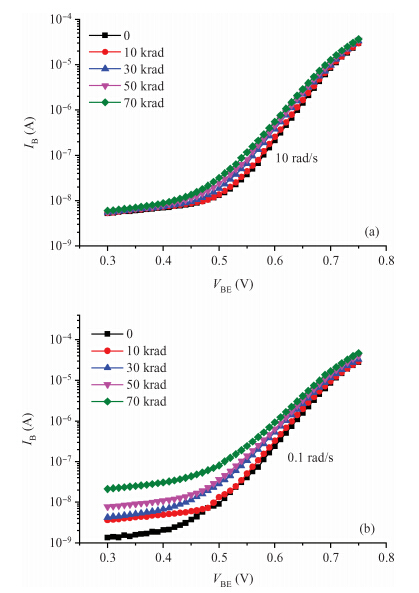
Ionizing-radiation-induced current gain degradation in NPN bipolar junction transistors is due to an increase in base current as a result of recombination at the surface of the device. A model is presented which identifies the physical mechanism responsible for current gain degradation. The increase in surface recombination velocity due to interface states results in an increase in base current. Besides, changing the surface potential along the base surface induced by the oxide-trapped charges can also lead to an increased base current. By combining the production mechanisms of oxide-trapped charges and interface states, this model can explain the fact that the current gain degradation is more severe at a low dose rate than at a high dose rate. The radiations were performed in a Co60 source up to a total dose of 70 krad(Si). The low dose rate was 0.1 rad(Si)/s and the high dose rate was 10 rad(Si)/s. The model accords well with the experimental results.

J. Semicond.
2015, 36(6): 064008 doi: 10.1088/1674-4926/36/6/064008

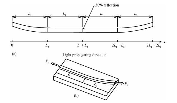
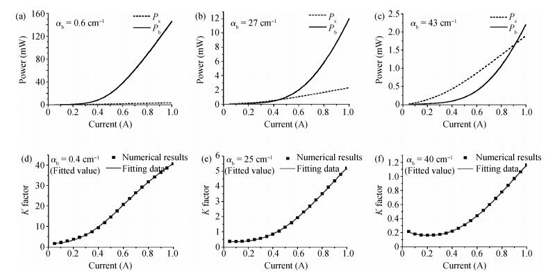
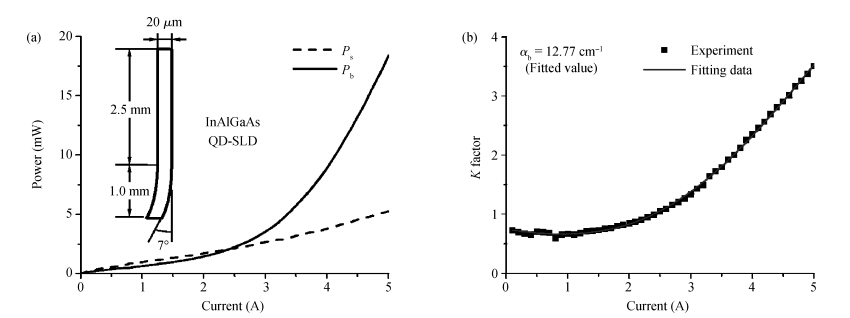
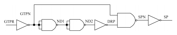
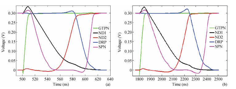
The optical loss in the bent region is one of the key features for bent-waveguide superluminescent diodes that affects the device performance greatly under some conditions. For the purpose of device fabrication and optimization, it will be helpful if this bend loss can be estimated. In this letter, we have derived an analytical formula which can be used to get the bend-loss coefficient by fitting the P-I curves of the devices. It is proved that the formula is successful in estimating the loss coefficients from the P-I curves simulated from a complicated quantum-dot device model. We expect this method could also be valid in estimating bend losses of actual devices.
J. Semicond.
2015, 36(6): 064009 doi: 10.1088/1674-4926/36/6/064009

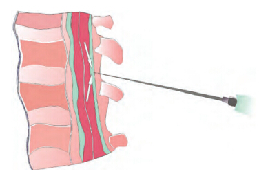
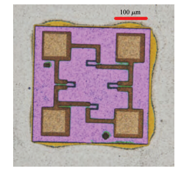
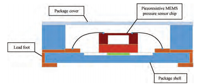
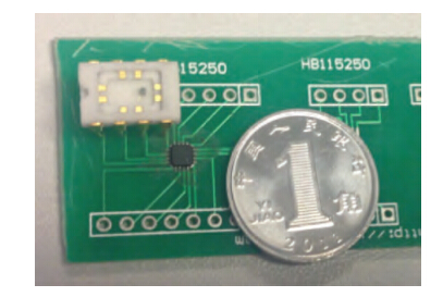
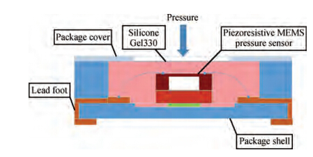
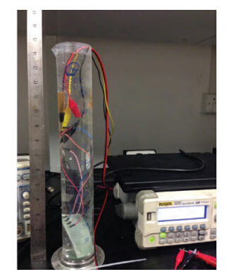
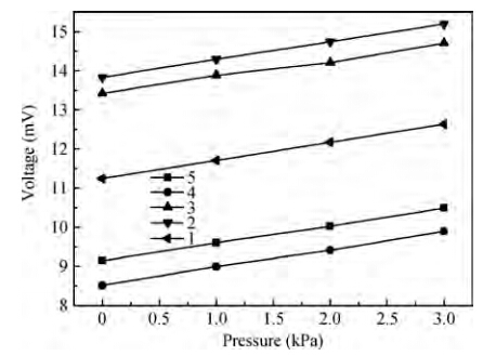
This paper presents a micro packaged MEMS pressure sensor for intracranial pressure measurement which belongs to BioMEMS. It can be used in lumbar puncture surgery to measure intracranial pressure. Miniaturization is key for lumbar puncture surgery because the sensor must be small enough to allow it be placed in the reagent chamber of the lumbar puncture needle. The size of the sensor is decided by the size of the sensor chip and package. Our sensor chip is based on silicon piezoresistive effect and the size is 400 × 400 μm2. It is much smaller than the reported polymer intracranial pressure sensors such as liquid crystal polymer sensors. In terms of package, the traditional dual in-line package obviously could not match the size need, the minimal size of recently reported MEMS-based intracranial pressure sensors after packaging is 10 × 10 mm2. In this work, we are the first to introduce a quad flat no-lead package as the package form of piezoresistive intracranial pressure sensors, the whole size of the sensor is minimized to only 3 × 3 mm2. Considering the liquid measurement environment, the sensor is gummed and waterproof performance is tested; the sensitivity of the sensor is 0.9 × 10⁻² mV/kPa.


J. Semicond.
2015, 36(6): 064010 doi: 10.1088/1674-4926/36/6/064010

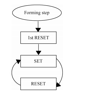
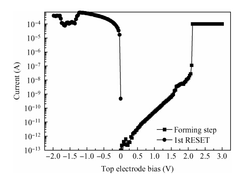
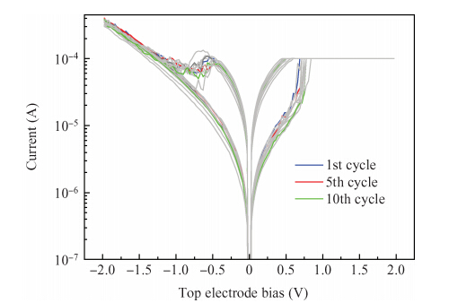
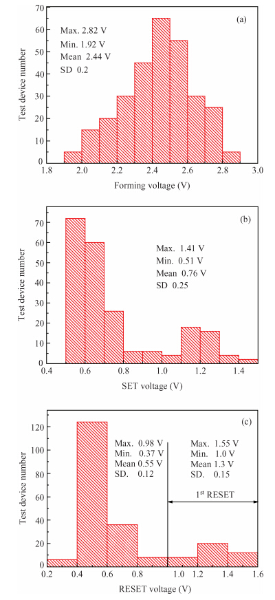
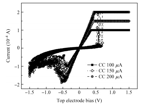
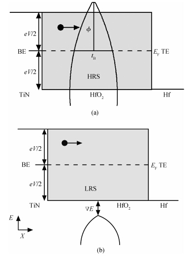
Nano-scale Hf/HfO2-based resistive random-access-memory (RRAM) devices were fabricated. The cross-over between top and bottom electrodes of RRAM forms the metal-insulator-metal sandwich structure. The electrical responses of RRAM are studied in detail, including forming process, SET process and RESET process. The correlations between SET voltage and RESET voltage, high resistance state and low resistance state are discussed. The electrical characteristics of RRAM are in a strong relationship with the compliance current in the SET process. The conduction mechanism of nano-scale Hf/HfO2-based RRAM can be explained by the quantum point contact model.

J. Semicond.
2015, 36(6): 064011 doi: 10.1088/1674-4926/36/6/064011

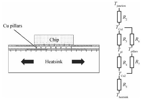
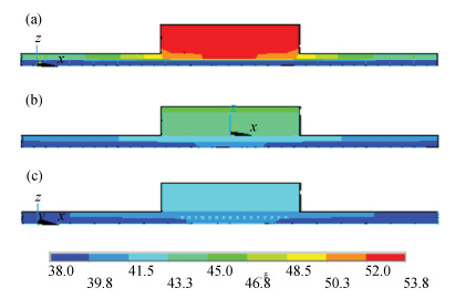
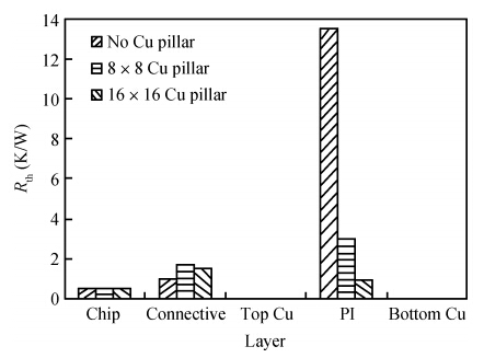
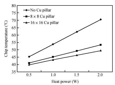
Chip on flexible substrate (COF) is a new packaging technology for light emitting diodes (LED). This paper investigated the effect of Cu-pillar in the polyimide (PI) layer on the thermal properties of COF LED packages by finite element analysis. The thermal distribution and thermal resistance were studied in both COF LED packages with and without Cu-pillar. The PI layer showed the highest thermal resistance in the typical package and led to a high chip temperature. With the addition of Cu-pillars, however, the thermal resistance of the PI layer significantly decreased due to the improvement of vertical thermal dissipation under LED chips. Based on the results of simulation and calculation, the relationship between the amount of Cu-pillar and thermal resistance of the COF package has been built. For the packages studied in this research, an 8 × 8 Cu-pillars array was adequate to improve the thermal performance of COF packages.


J. Semicond.
2015, 36(6): 064012 doi: 10.1088/1674-4926/36/6/064012

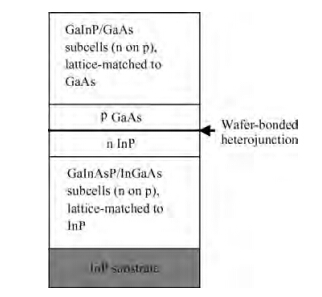
Direct wafer bonding technology is able to integrate two smooth wafers and thus can be used in fabricating III-V multijunction solar cells with lattice mismatch. In order to monolithically interconnect between the GaInP/GaAs and InGaAsP/InGaAs subcells, the bonded GaAs/InP heterojunction must be a highly conductive ohmic junction or a tunnel junction. Three types of bonding interfaces were designed by tuning the conduction type and doping elements of GaAs and InP. The electrical properties of p-GaAs (Zn doped)/n-InP (Si doped), p-GaAs (C doped)/n-InP (Si doped) and n-GaAs (Si doped)/n-InP (Si doped) bonded heterojunctions were analyzed from the I-V characteristics. The wafer bonding process was investigated by improving the quality of the sample surface and optimizing the bonding parameters such as bonding temperature, bonding pressure, bonding time and so on. Finally, GaInP/GaAs/InGaAsP/InGaAs 4-junction solar cells have been prepared by a direct wafer bonding technique with the high efficiency of 34.14% at the AM0 condition (1 Sun).


J. Semicond.
2015, 36(6): 064013 doi: 10.1088/1674-4926/36/6/064013

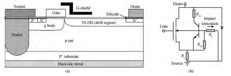
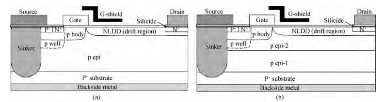
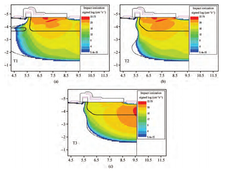
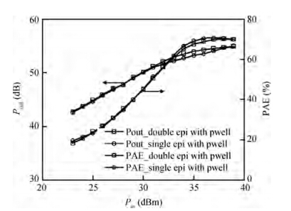
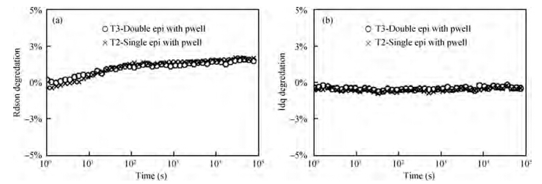
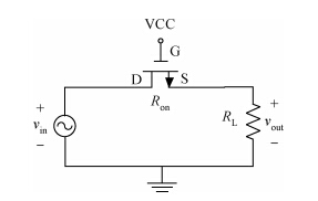
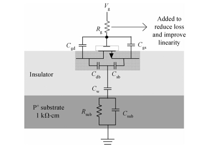
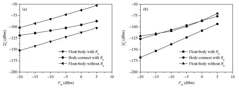
A laterally diffused metal-oxide-semiconductor (LDMOS) device design with an enhanced p-well and double p-epitaxial structure is investigated for device ruggedness improvement while keeping its high device performance under high frequency. Based upon the device design, radio-frequency (RF) LDMOS transistors for GSM (global system for mobile communication) application have been fabricated by using 0.35 μm CMOS technologies. Experimental data show that the proposed device achieves a breakdown voltage of 70 V, output power of 180 W. The RF linear gain is over 20 dB and the power added efficiency (PAE) is over 70% with the frequency of 920 MHz. In particular, it can pass the 20 : 1 voltage standing wave ratio (VSWR) load mismatch biased at drain DC supply voltage of 32 V and output power at 10-dB gain compression point (P10dB). The device ruggedness has been remarkably improved by using the proposed device structure.


J. Semicond.
2015, 36(6): 065001 doi: 10.1088/1674-4926/36/6/065001

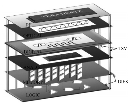
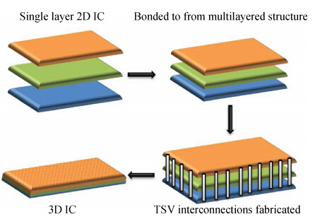
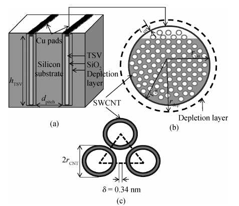
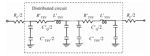
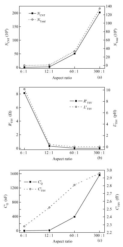
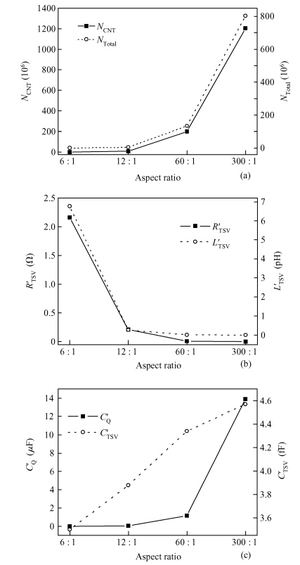
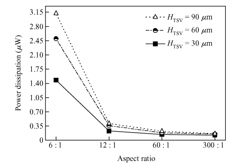
Through-silicon vias (TSVs) have provided an attractive solution for three-dimensional (3D) integrated devices and circuit technologies with reduced parasitic losses and power dissipation, higher input-output (I/O) density and improved system performance. This paper investigates the propagation delay and average power dissipation of single-walled carbon nanotube bundled TSVs having different via radius and height. Depending on the physical configuration, a comprehensive and accurate analytical model of CNT bundled TSV is employed to represent the via (vertical interconnect access) line of a driver-TSV-load (DTL) system. The via radius and height are used to estimate the bundle aspect ratio (AR) and the cross-sectional area. For a fixed via height, the delay and the power dissipation are reduced up to 96.2% using a SWCNT bundled TSV with AR = 300 : 1 in comparison to AR = 6 : 1.


J. Semicond.
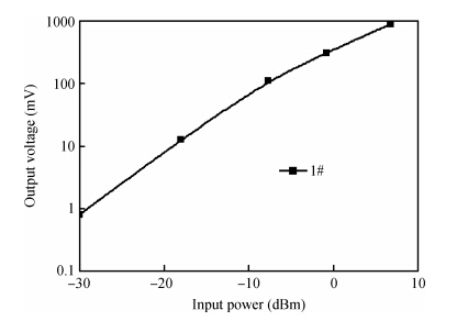
2015, 36(6): 065002 doi: 10.1088/1674-4926/36/6/065002

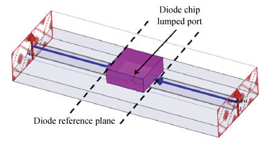
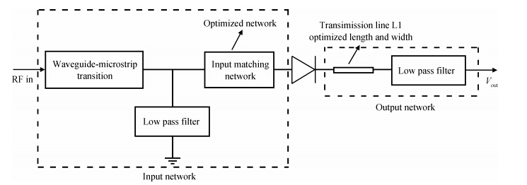
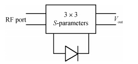
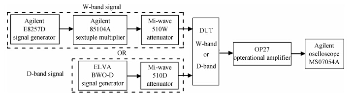
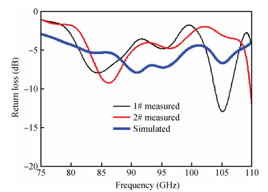
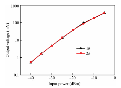
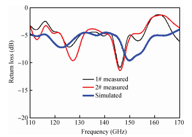
Two broadband detectors at W-band and D-band are analyzed and designed with low barrier Schottky diodes. The input circuit of the detectors is realized by low and high impedance microstrip lines, and their output circuit is composed of a radio frequency (RF) bandstop filter and a tuning line for optimum reflection phase of the RF signal. S-parameters of the complete circuit are exported to a circuit simulator for voltage sensitivity analysis. For the W band detectors, the highest measured voltage sensitivity is 11800 mV/mW at 100 GHz, and the sensitivity is higher than 2000 mV/mW in 80-104 GHz. Measured tangential sensitivity (TSS) is higher than-38 dBm, and its linearity is superior than 0.99992 at 95 GHz. For the D band detector, the highest measured voltage sensitivity is 1600 mV/mW, and the typical sensitivity is 600 mV/mW in 110-170 GHz. TSS is higher than-29 dBm, and its linearity is superior than 0.99961 at 150 GHz.


J. Semicond.
2015, 36(6): 065003 doi: 10.1088/1674-4926/36/6/065003

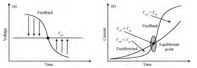
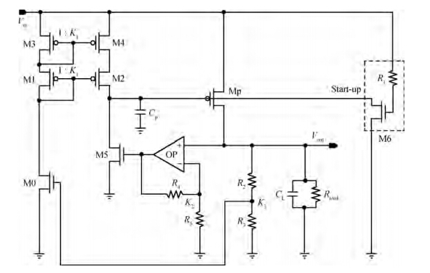
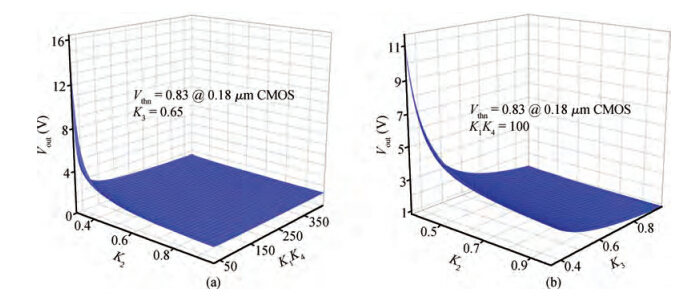
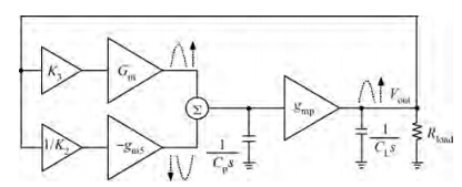
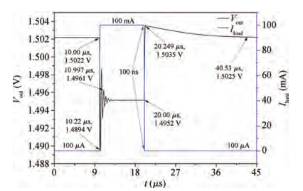
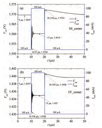
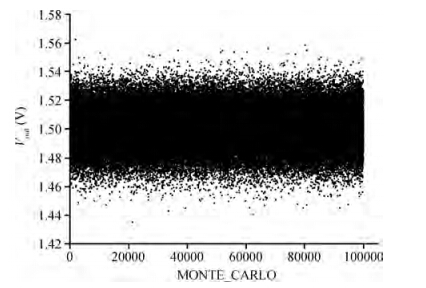
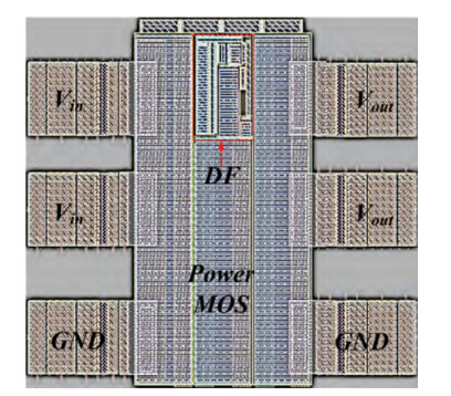
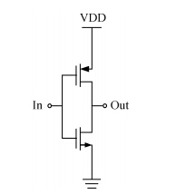
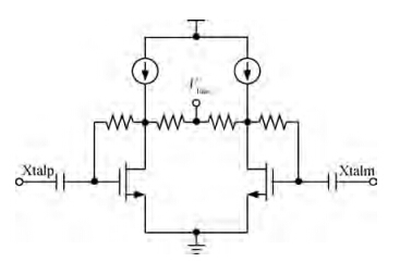
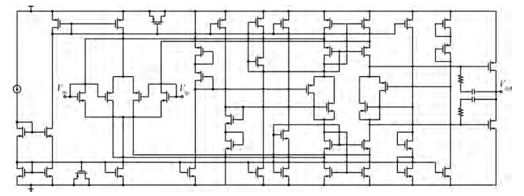
A novel dual-feed (DF) low-dropout (LDO) is presented. The DF-LDO adopts dual control loops to maintain the output voltage. The dual control loops include a feedback loop and a feedforward loop. There is an equilibrium point in dual control loops, and the equilibrium point is the output voltage of the DF-LDO. In addition, the transient performance is optimized by adjusting the damping ratio and natural frequency. With a 1 μF decoupling capacitor, the proposed DF-LDO is fabricated in a 0.18 μm CMOS process and its output voltage is 1.5 V. When the workload changes from 100 μA to 100 mA in 100 ns, load regulation of 7 mV for a 100 mA step is achieved, the settling time is 997 ns and the undershoot is 12.8 mV; when the workload changes from 100 mA to 100 μA in 100 ns, the settling time is 249 ns with an imperceptible overshoot.

J. Semicond.
2015, 36(6): 065004 doi: 10.1088/1674-4926/36/6/065004

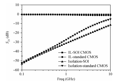
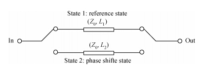
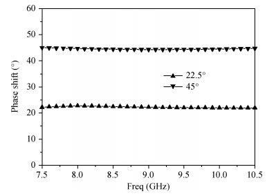
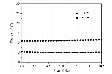
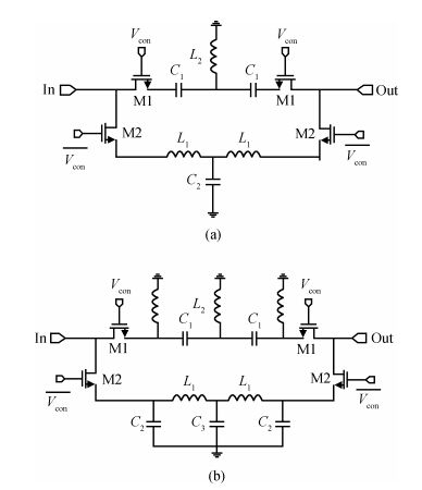
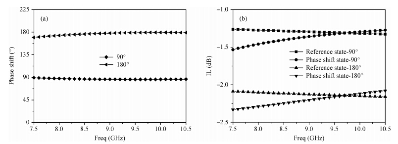
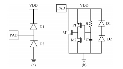
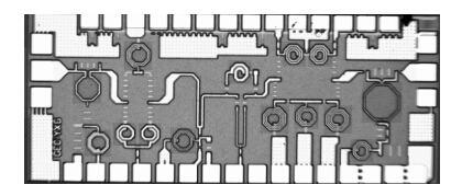
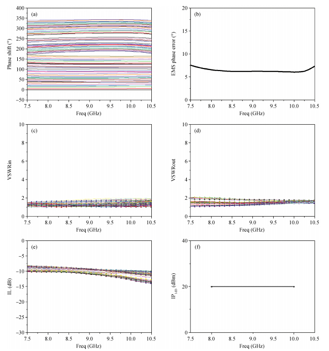
This paper proposed an X-band 6-bit passive phase shifter (PS) designed in 0.18 μm silicon-on-insulator (SOI) CMOS technology, which solves the key problem of high integration degree, low power, and a small size T/R module. The switched-topology is employed to achieve broadband and flat phase shift. The ESD circuit and driver are also integrated in the PS. It covers the frequency band from 7.5 to 10.5 GHz with an EMS phase error less than 7.5°. The input and output VSWRs are less than 2 and the insertion loss (IL) is between 8-14 dB across the 7.5 to 10.5 GHz, with a maximum IL difference of 4 dB. The input 1 dB compression point (IP 1dB) is 20 dBm.


J. Semicond.
2015, 36(6): 065005 doi: 10.1088/1674-4926/36/6/065005

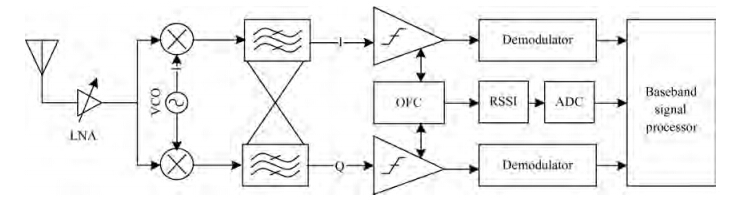
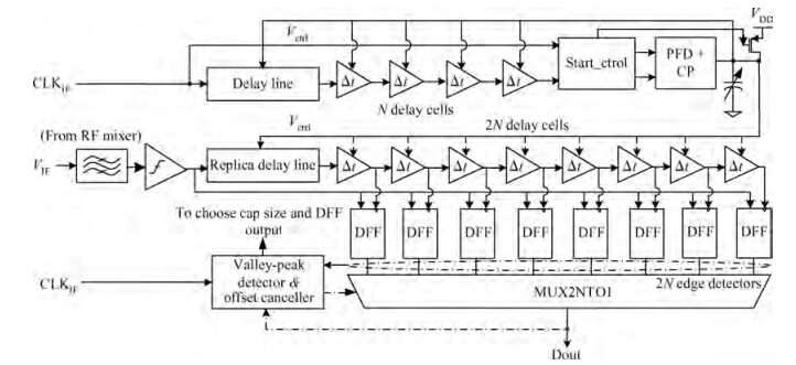
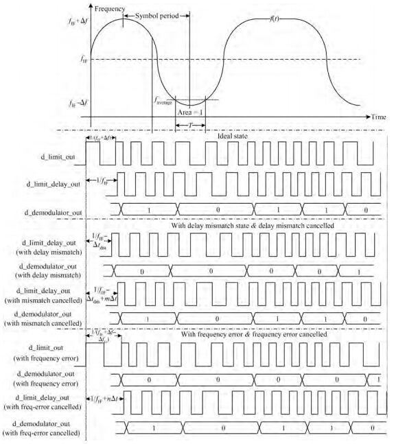
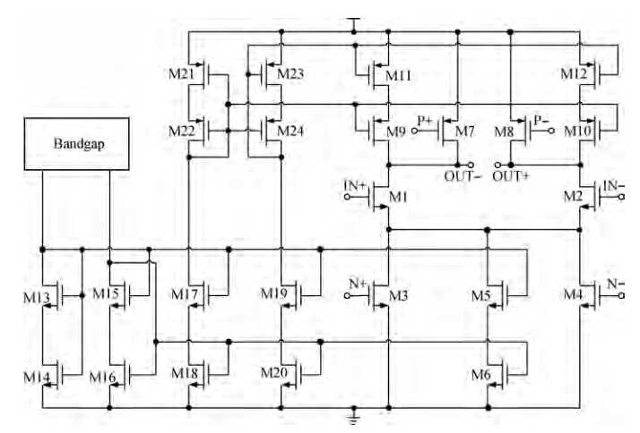
This paper presents a low power, high sensitivity Gaussian frequency shift keying (GFSK) demodulator with a flexible frequency offset canceling method for wireless networks for industrial automation process automation (WIA-PA) transceiver fabricated in 0.18 μm CMOS technology. The receiver uses a low-IF (1.5 MHz) architecture, and the transmitter uses a sigma delta PLL based modulation with Gaussian low-pass filter for low power consumption. The active area of the demodulator is 0.14 mm2. Measurement results show that the proposed demodulator operates without harmonic distortion, deals with ± 180 kHz frequency offset, needs SNR only 18.5 dB at 0.1% bit-error rate (BER), and consumes no more than 0.26 mA from a 1.8 V power supply.


J. Semicond.
2015, 36(6): 065006 doi: 10.1088/1674-4926/36/6/065006

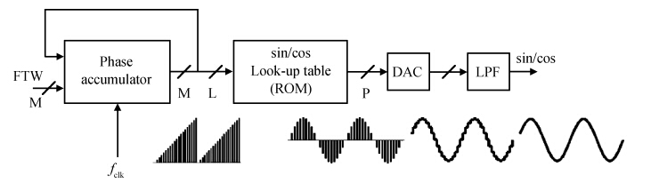
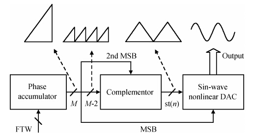
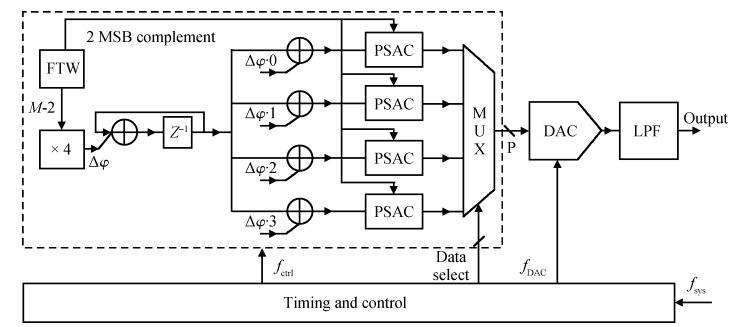
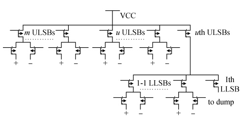
This paper presents a direct digital frequency synthesizer (DDFS) for high speed application based on multi-channel structure. This DDFS has phase resolution of 32 bits and magnitude resolution of 12 bits. In order to ensure the high speed and high resolution at the same time, the multi-channel sampling technique is used and a 12 bits linear digital-to-analog converter is implemented. The chip is fabricated in TSMC 130 nm CMOS technology with active area of 0.89 × 0.98 mm2 and total power consumption of 300 mW at a single 1.2 V supply voltage. The maximum operating speed is up to 2.0 GHz at room temperature.

J. Semicond.
2015, 36(6): 065007 doi: 10.1088/1674-4926/36/6/065007

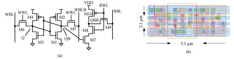
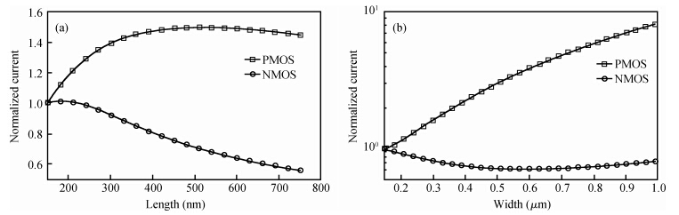
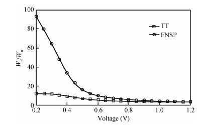
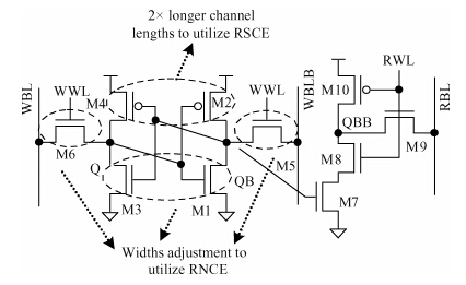
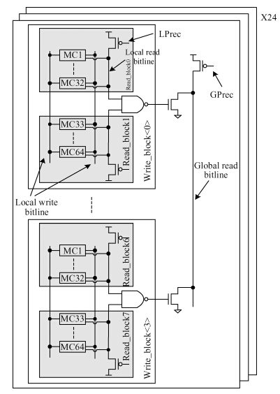
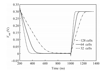
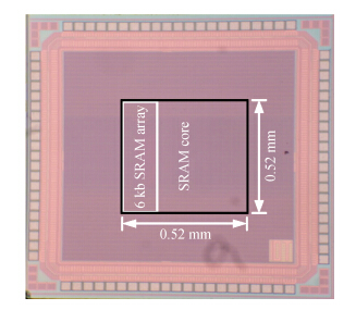
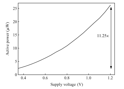
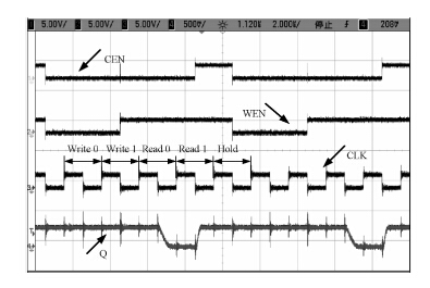
This paper presents a 6 kb SRAM that uses a novel 10T cell to achieve a minimum operating voltage of 320 mV in a 130 nm CMOS process. A number of low power circuit techniques are included to enable the proposed SRAM to operate in the subthreshold region. The reverse short channel effect and the reverse narrow channel effect are utilized to improve the performance of the SRAM. A novel subthreshold pulse generation circuit produces an ideal pulse to make read operation stable. A floating write bit-line effectively reduces the standby leakage consumption. Finally, a short read bit-line makes the read operation fast and energy-saving. Measurements indicate that these techniques are effective, the SRAM can operate at 800 kHz and consume 1.94 μW at its lowest voltage (320 mV).
J. Semicond.
2015, 36(6): 065008 doi: 10.1088/1674-4926/36/6/065008

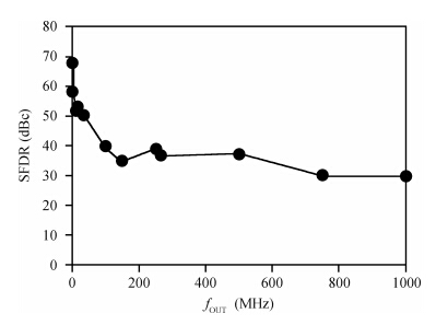
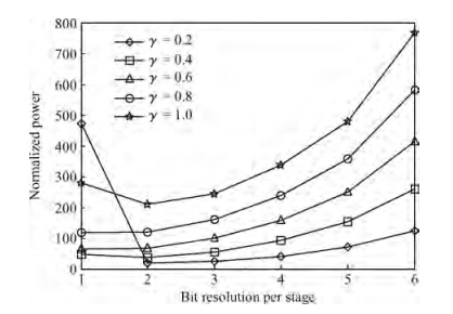
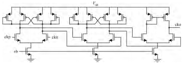
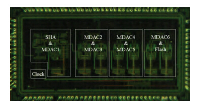
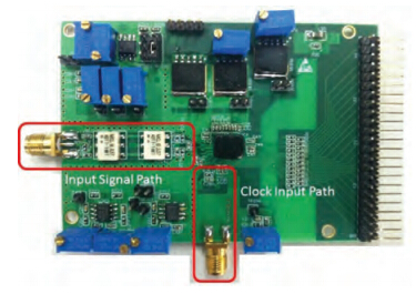
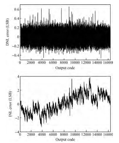
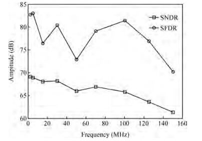
This paper presents a high-speed high-resolution pipelined ADC with low power and small area. The proposed ADC is designed based on the analysis of the stage scaling theory and the residual amplifiers are shared by two cascading MDACs to reduce power consumption. Shared op-amps with two split input paths are presented in this paper to eliminate the nonlinearity effects such as memory effect and crosstalk. Dynamic pre-amplified comparators are employed to decrease the static power consumption and suppress the kick-back in the comparators. This ADC is implemented in SMIC 0.18 μm CMOS process with an area of 3.1 mm2. With a sampling rate of 100 MS/s, spurious-free dynamic range (SFDR) and signal-to-noise plus distortion ratio (SNDR) of the ADC are 82.7 dB and 69.1 dB, respectively. For signals up to 100 MHz, the SFDR and SNDR achieve 81.4 dB and 65.8 dB. The power consumption is 121 mW with a 1.8 V supply voltage.


J. Semicond.
2015, 36(6): 065009 doi: 10.1088/1674-4926/36/6/065009

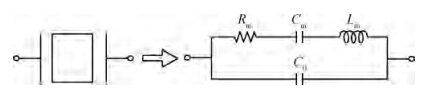
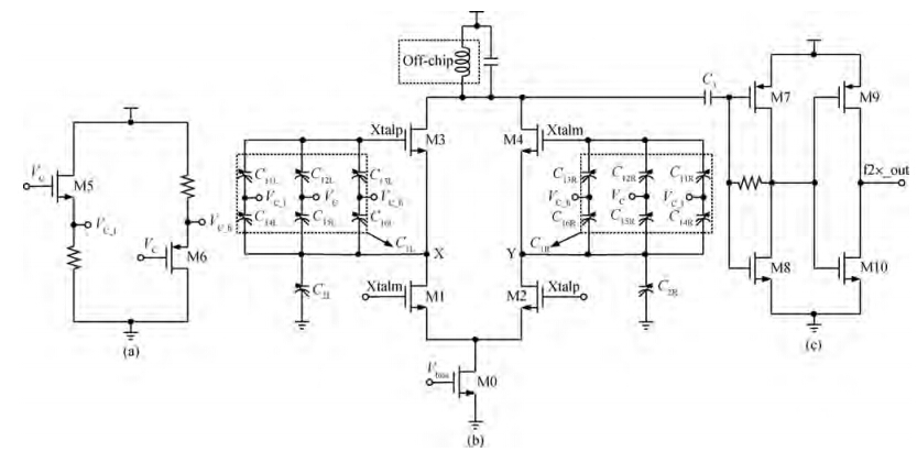
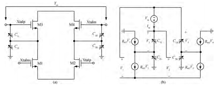
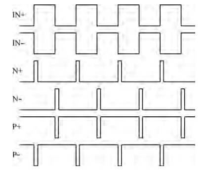
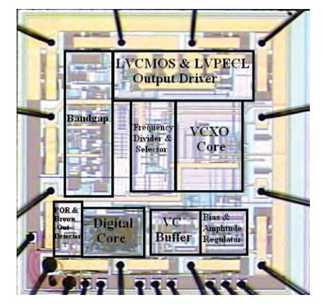
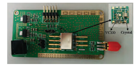
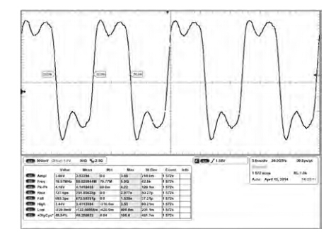
This paper describes a low phase noise, wide tuning range and high tuning linearity CMOS voltage controlled crystal oscillator IC (VCXO-IC) with LVCMOS or LVPECL output. A differential coupled frequency doubling Colpitts oscillator is adopted to obtain low noise 2 × frequency output. A wide tuning range and high linearity are simultaneously achieved by using MOS varactor arrays. The measurement results show that the designed VCXO-IC achieves-134 dBc/Hz phase noise at 1 kHz offset frequency and ± 135 ppm output frequency tuning range within 3% linearity by using 40 MHz fundamental AT-cut crystal. The VCXO-IC is fabricated in the chartered 0.35 μm standard CMOS process and occupies a total silicon area of 2.4 mm2.


J. Semicond.
2015, 36(6): 065010 doi: 10.1088/1674-4926/36/6/065010

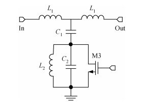
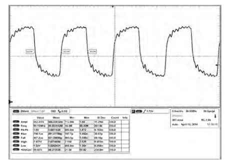
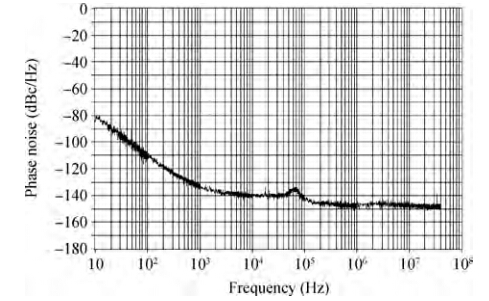
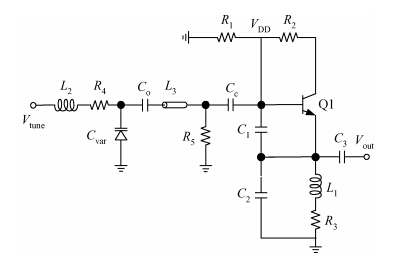
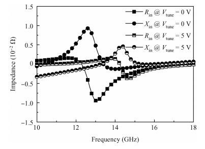
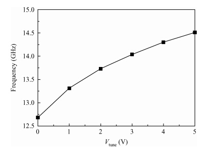
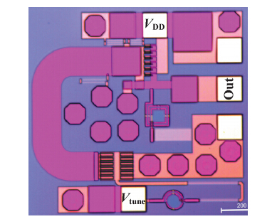
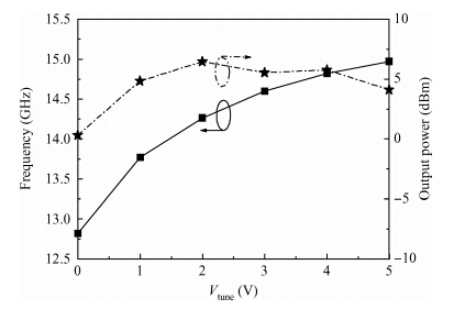
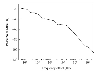
A fully integrated Ku-band voltage controlled oscillator (VCO) is presented in an InGaP/GaAs heterojunction bipolar transistor (HBT) technology. To achieve the wide tuning range (TR), the VCO employs a Colpitts configuration, and the VCO simultaneously achieves high output power. The implemented VCO demonstrates an oscillation frequency range from 12.82 to 14.97 GHz, a frequency TR of 15.47%, an output power from 0.31 to 6.46 dBm, and a phase noise of-94.9 dBc/Hz at 1 MHz offset from 13.9 GHz center frequency. The VCO consumes 52.75 mW from 5 V supply and occupies an area of 0.81 × 0.78 mm2. Finally, the figures-of-merit for VCOs is discussed.

J. Semicond.
2015, 36(6): 066001 doi: 10.1088/1674-4926/36/6/066001

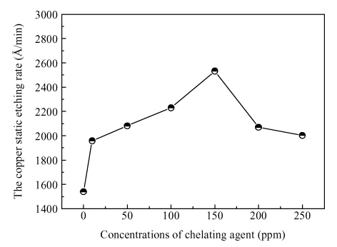
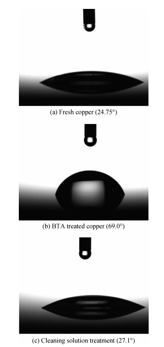
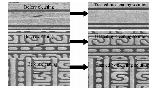
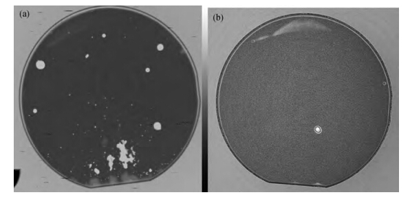
This work investigates systematically the effect of FA/O II chelating agent and FA/O I surfactant in alkaline cleaning solutions on benzotriazole (BTA) removal during post-Cu CMP cleaning in GLSI under the condition of static etching. The best detergent formulation for BTA removal can be determined by optimization of the experiments of single factor and compound cleaning solution, which has been further confirmed experimentally by contact angle (CA) measurements. The resulting solution with the best formulation has been measured for the actual production line, and the results demonstrate that the obtained cleaning solution can effectively and efficiently remove BTA, CuO and abrasive SiO2 without basically causing interfacial corrosion. This work demonstrates the possibility of developing a simple, low-cost and environmentally-friendly cleaning solution to effectively solve the issues of BTA removal on post-Cu CMP cleaning in a multi-layered copper wafer.