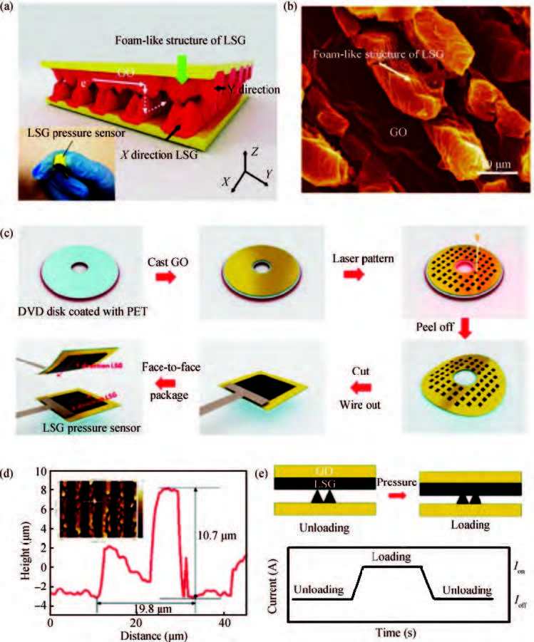
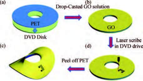
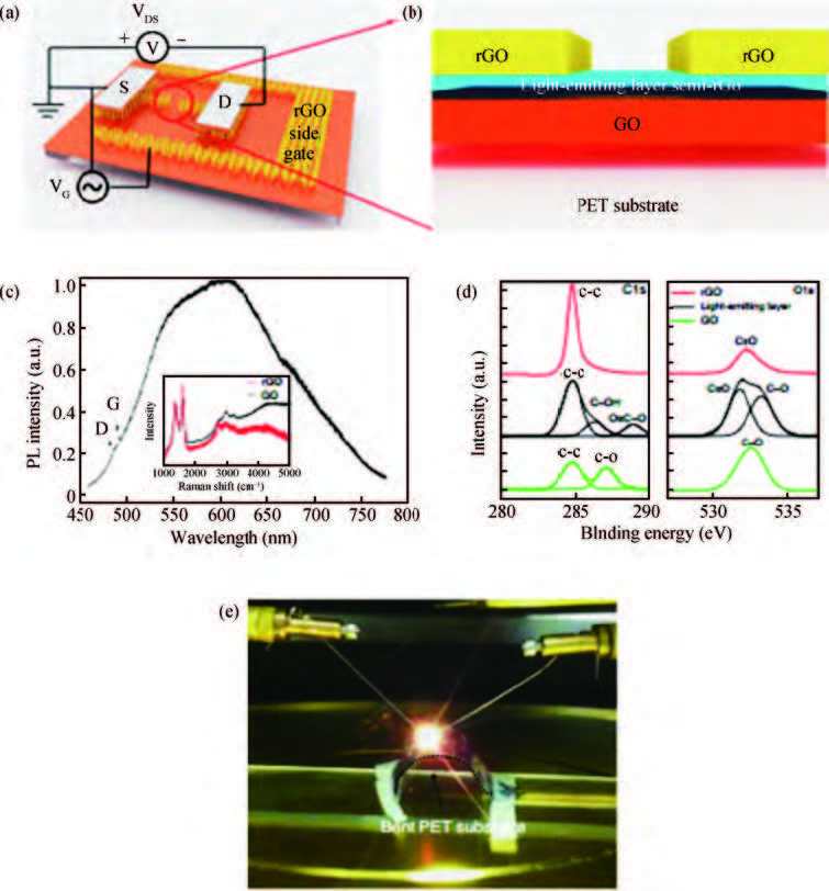
In recent years, flexible electronic devices have become a hot topic of scientific research. These flexible devices are the basis of flexible circuits, flexible batteries, flexible displays and electronic skins. Graphene-based materials are very promising for flexible electronic devices, due to their high mobility, high elasticity, a tunable band gap, quantum electronic transport and high mechanical strength. In this article, we review the recent progress of the fabrication process and the applications of graphene-based electronic devices, including thermal acoustic devices, thermal rectifiers, graphene-based nanogenerators, pressure sensors and graphene-based light-emitting diodes. In summary, although there are still a lot of challenges needing to be solved, graphene-based materials are very promising for various flexible device applications in the future.


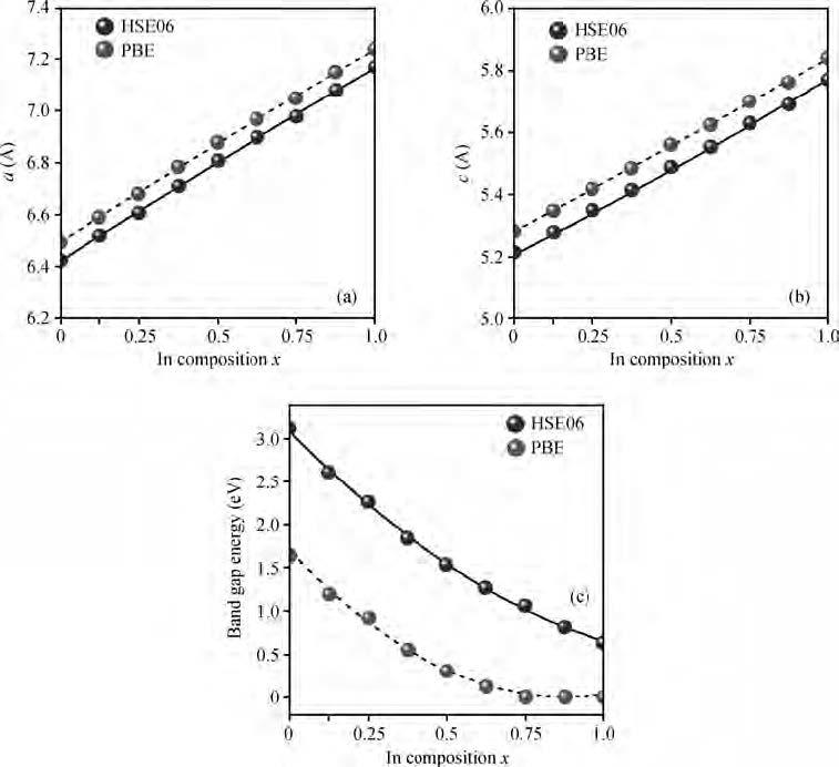
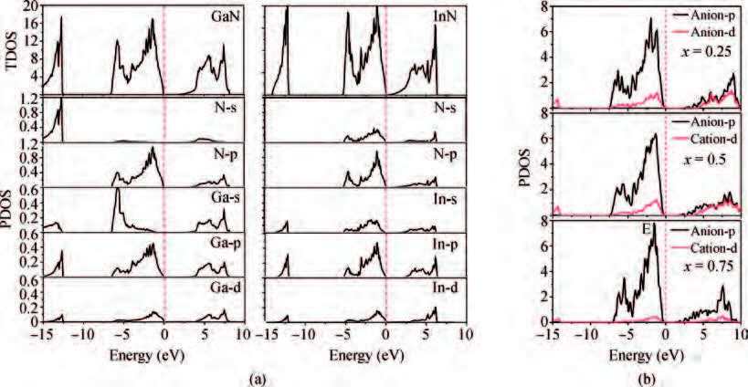
The electronic band structures and band gap bowing parameters of InxGa1-xN are studied by the first-principles method based on the density functional theory. Calculations by employing both the Heyd-Scuseria-Ernzerh of hybrid functional (HSE06) and the Perdew-Burke-Ernzerhof (PBE) one are performed. We found that the theoretical band gap bowing parameter is dependent significantly on the calculation method, especially on the exchange-correlation functional employed in the DFT calculations. The band gap of InxGa1-xN alloy decreases considerably when the In constituent x increases. It is the interactions of s-s and p-p orbitals between anions and cations that play significant roles in formatting the band gaps bowing. In general, the HSE06 hybrid functional could provide a good alternative to the PBE functional in calculating the band gap bowing parameters.

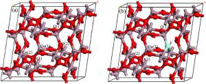
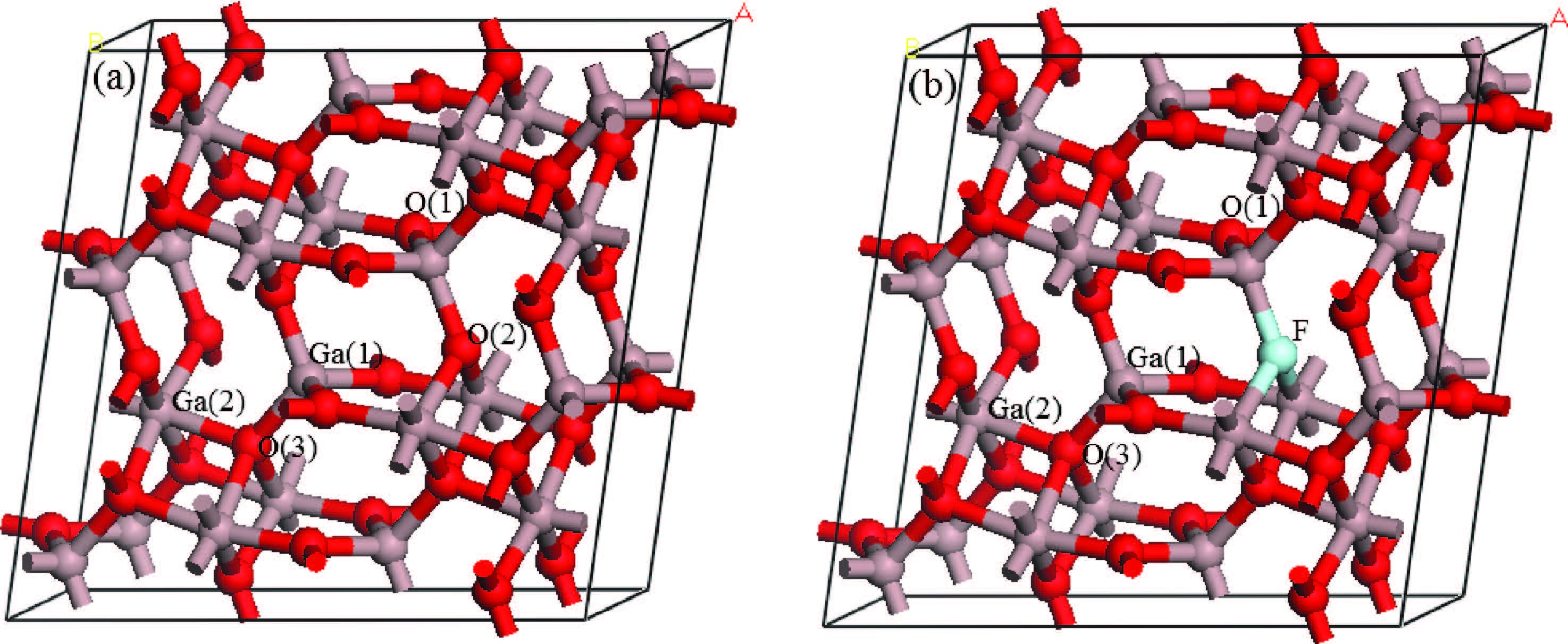
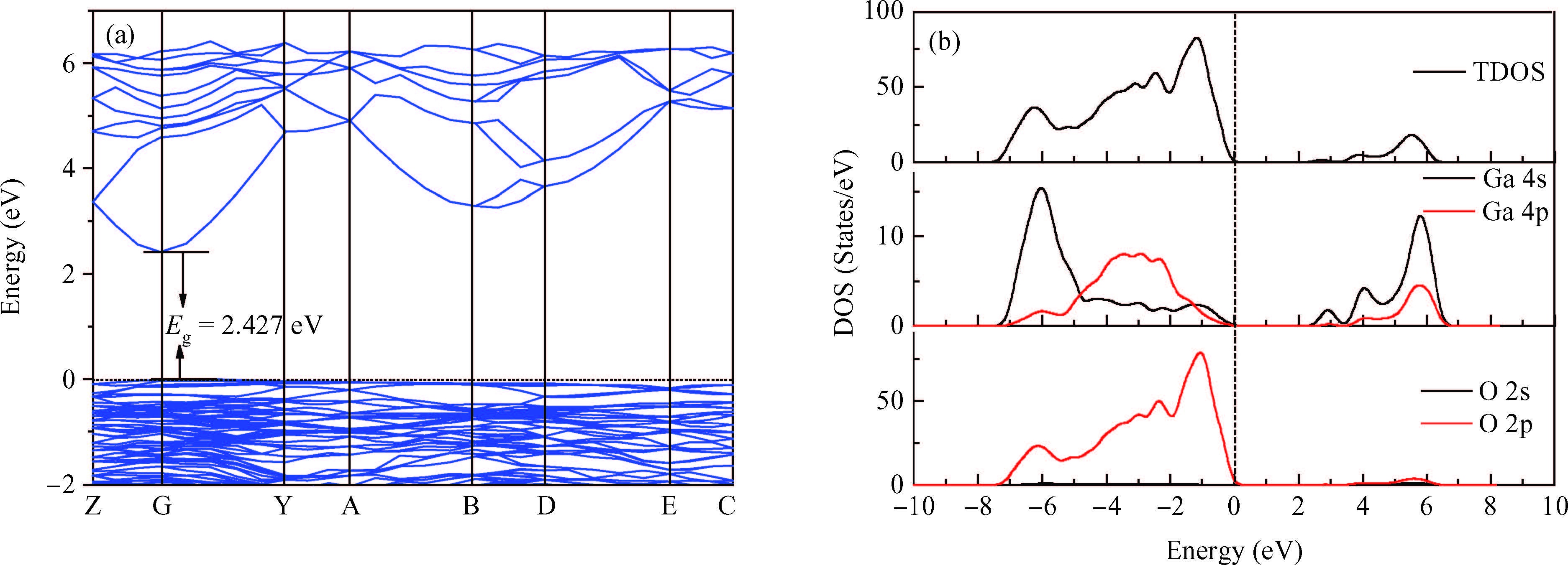
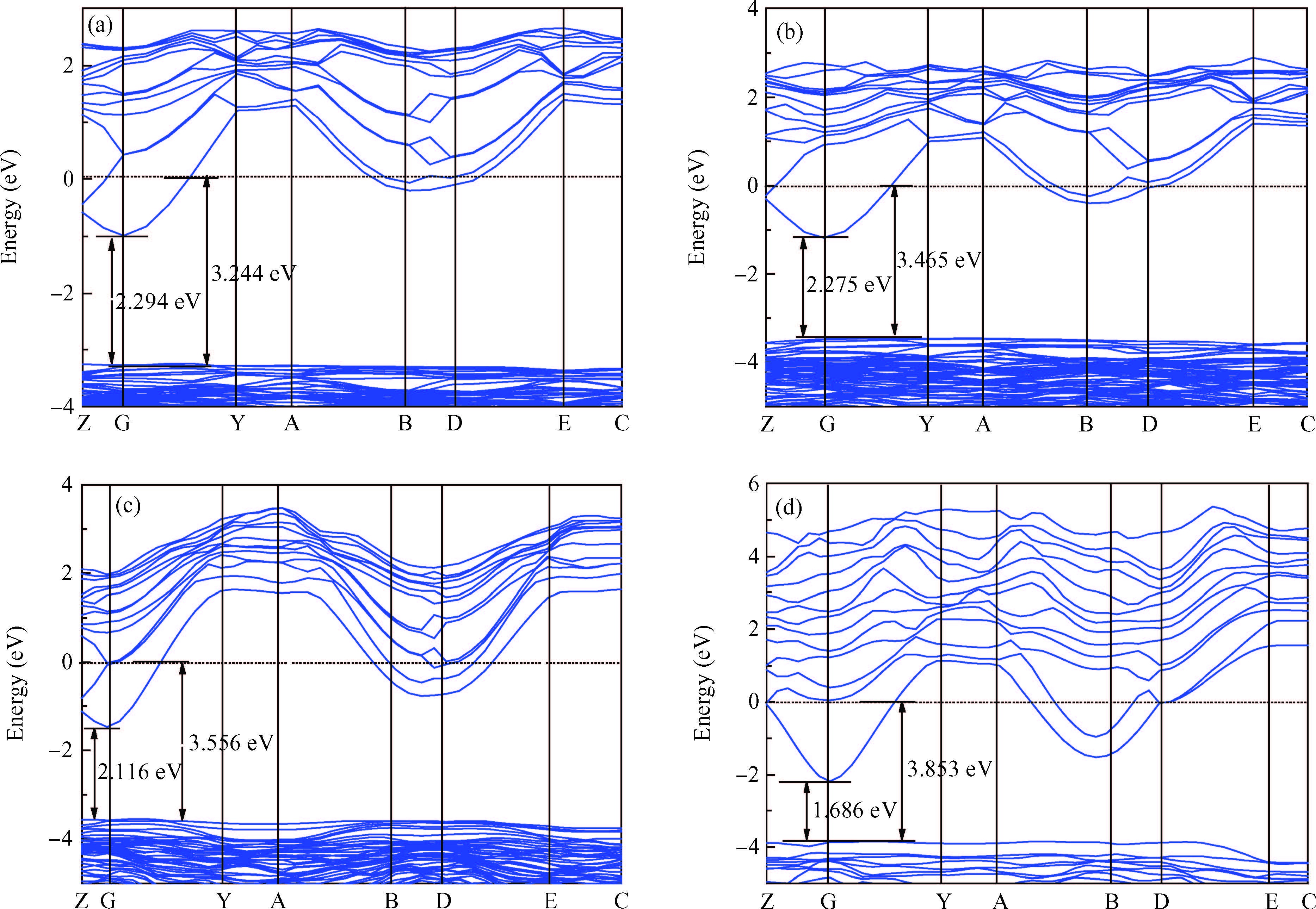
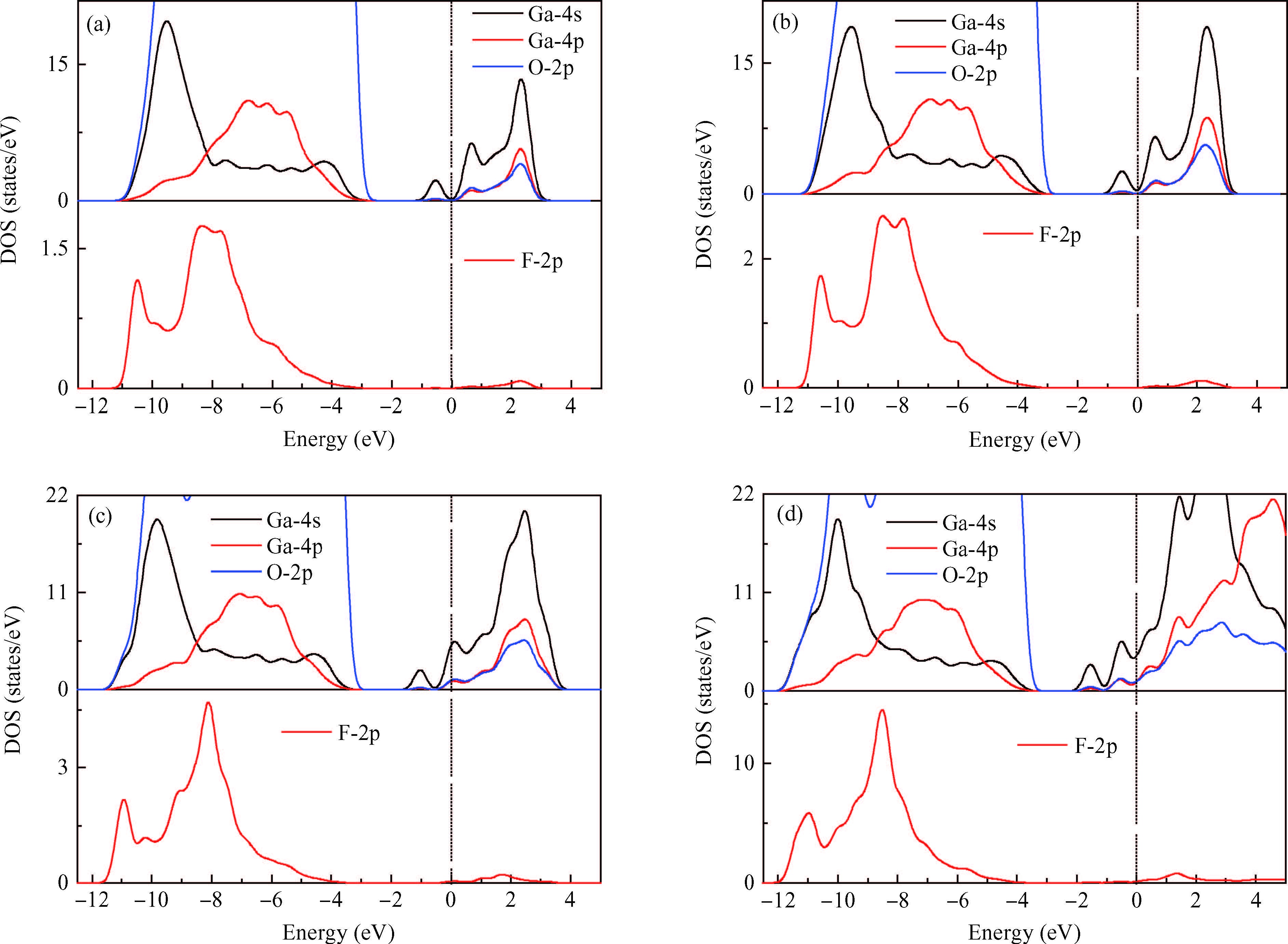
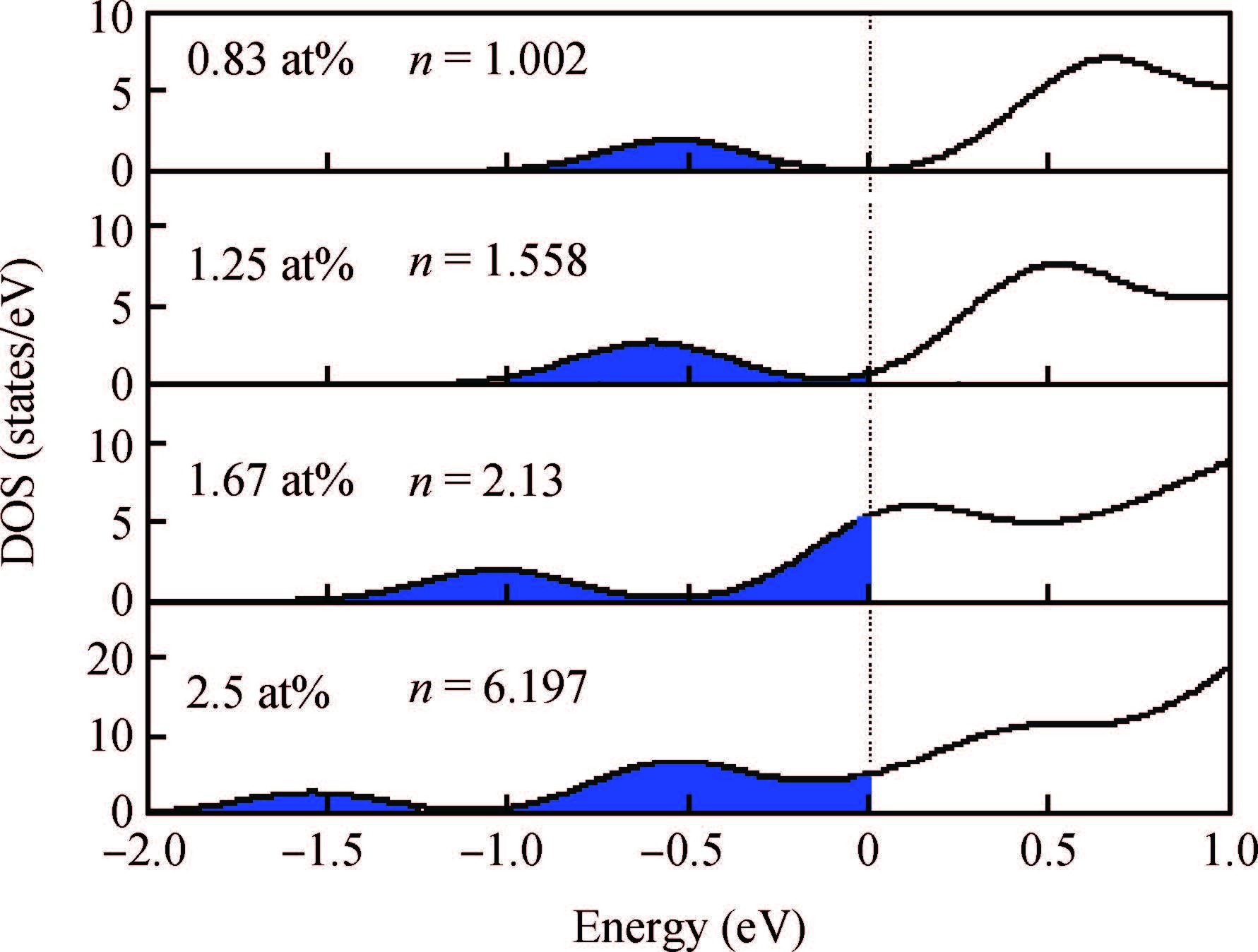
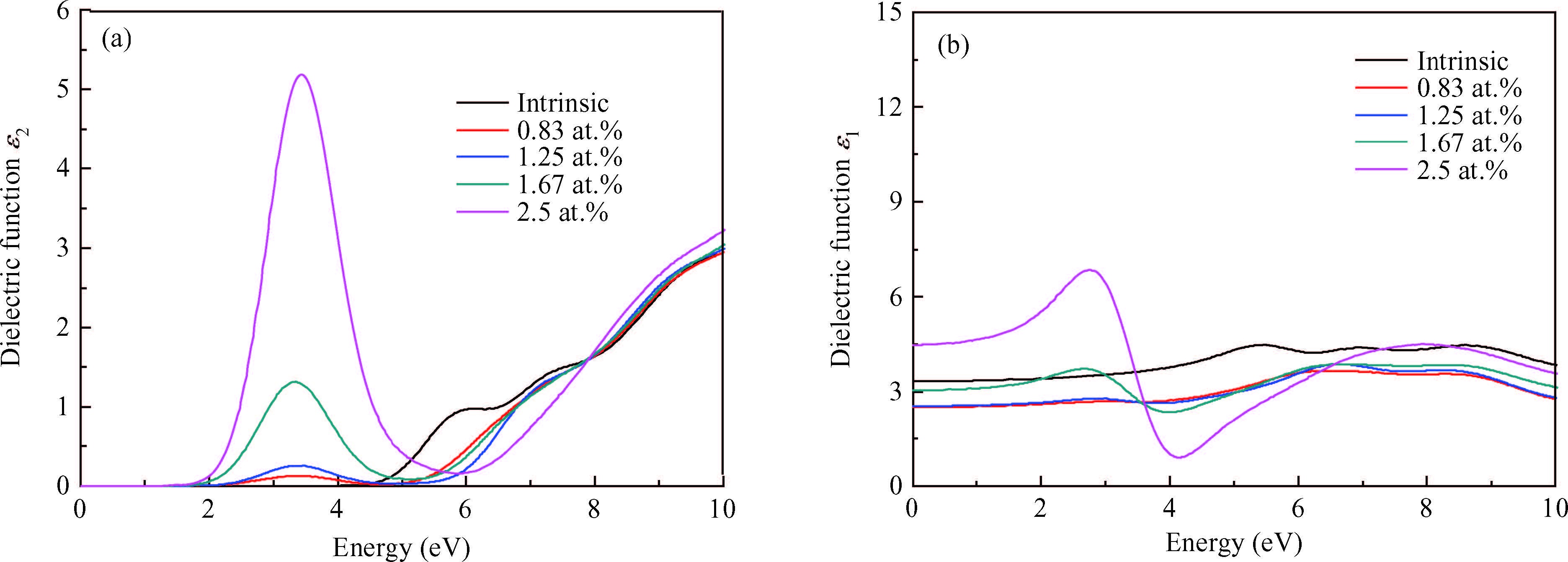
The effects of F-doping concentration on geometric structure, electronic structure and optical property of β-Ga2O3 were investigated. All F-doped β-Ga2O3 with different concentrations are easy to be formed under Ga-rich conditions, the stability and lattice parameters increase with the F-doping concentration. F-doped β-Ga2O3 materials display characteristics of the n-type semiconductor, occupied states contributed from Ga 4s, Ga 4p and O 2p states in the conduction band increase with an increase in F-doping concentration. The increase of F concentration leads to the narrowing of the band gap and the broadening of the occupied states. F-doped β-Ga2O3 exhibits the sharp band edge absorption and a broad absorption band. Absorption edges are blue-shifted, and the intensity of broad band absorption has been enhanced with respect to the fluorine content. The broad band absorption is ascribed to the intra-band transitions from occupied states to empty states in the conduction band.
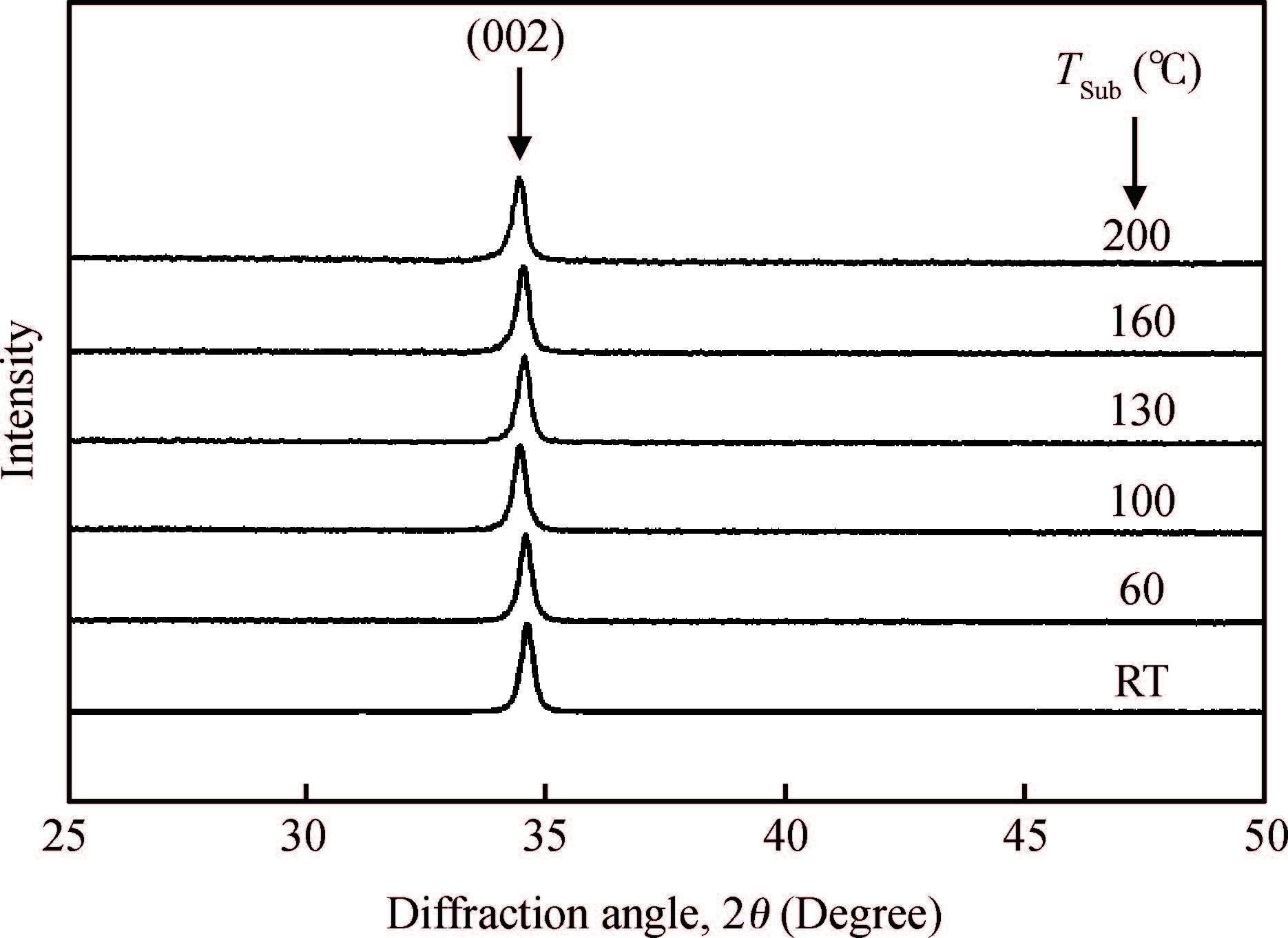
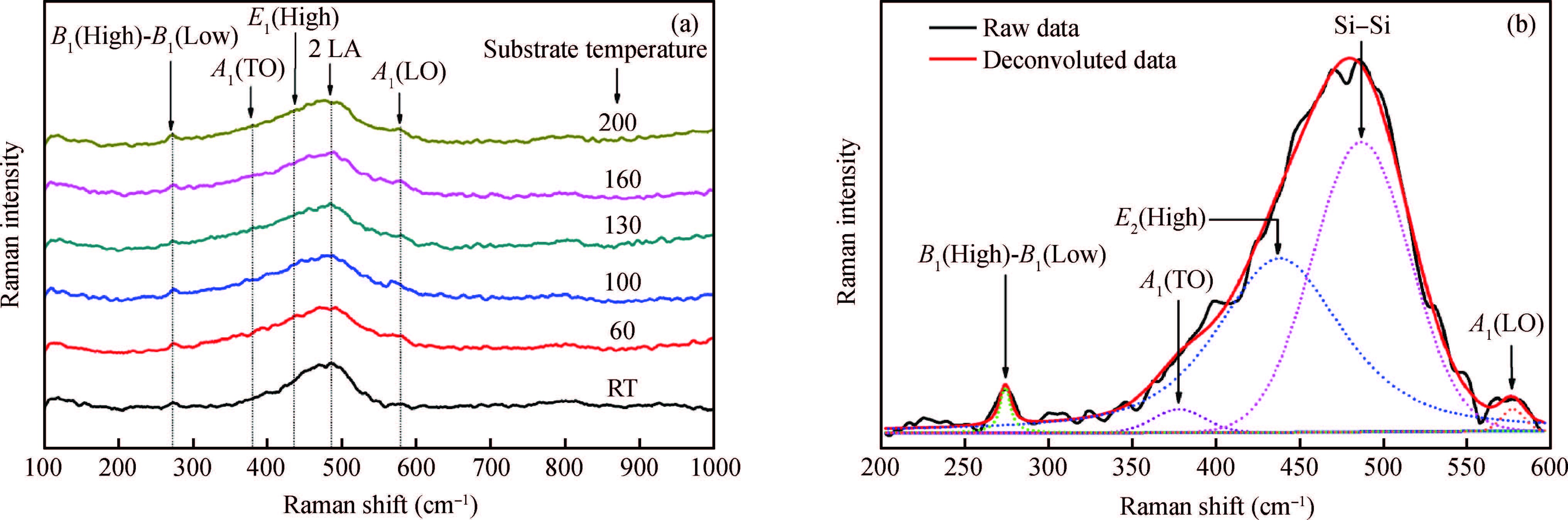
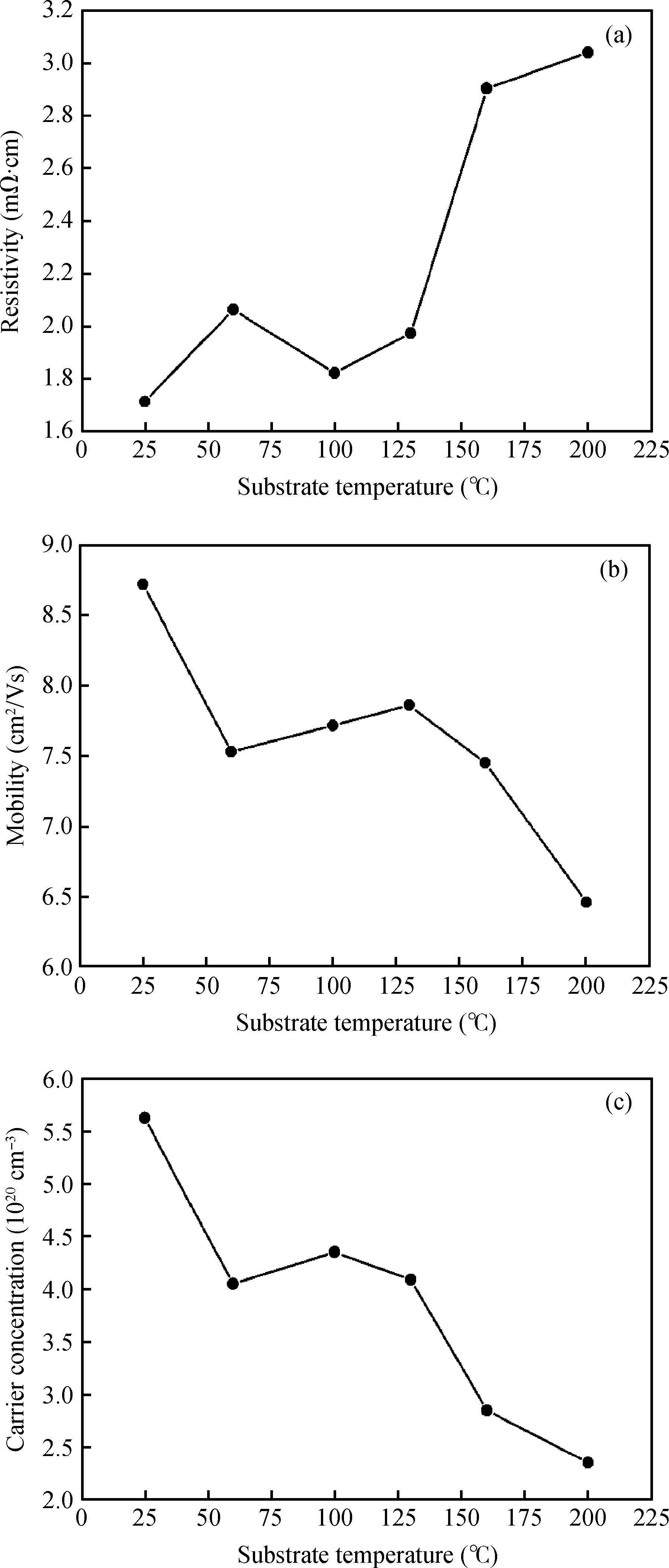
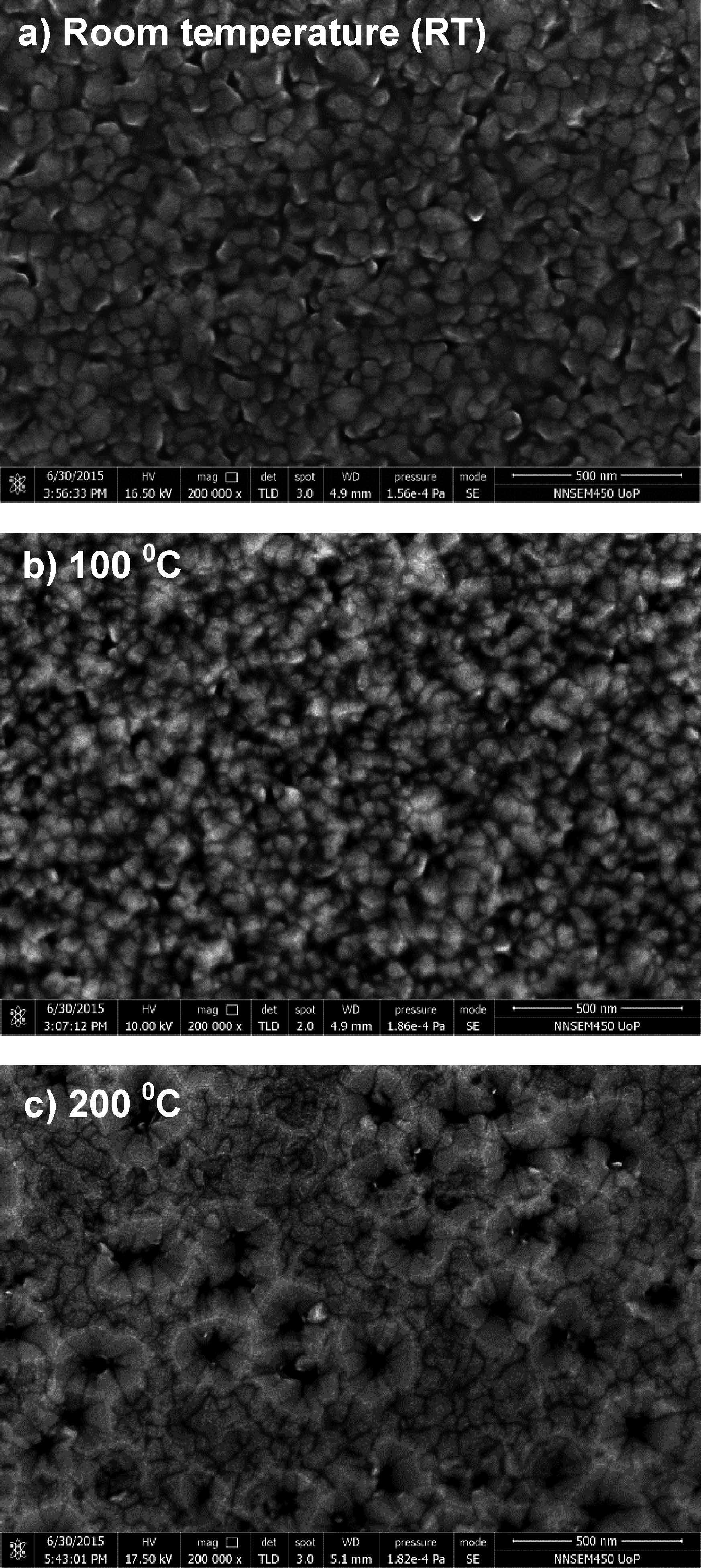
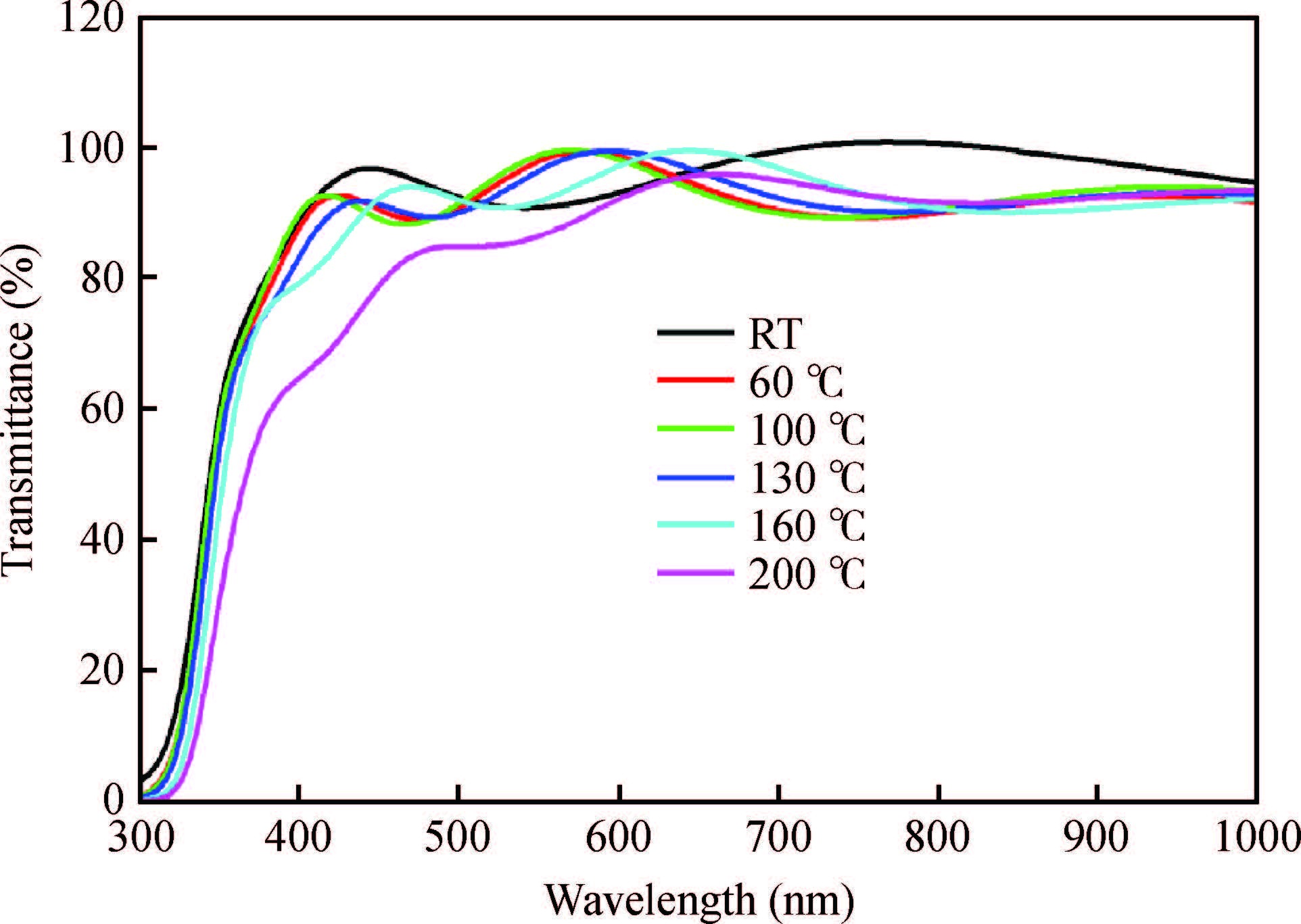
Transparent and conducting Al-doped ZnO (ZnO:Al) films were prepared on glass substrate using the RF sputtering method at different substrate temperatures from room temperature (RT) to 200℃. The structural, morphological, electrical and optical properties of these films were investigated using a variety of characterization techniques such as low angle XRD, Raman spectroscopy, X-ray photoelectron spectroscopy (XPS), field-emission scanning electron microscopy (FE-SEM), Hall measurement and UV-visible spectroscopy. The electrical properties showed that films deposited at RT have the lowest resistivity and it increases with an increase in the substrate temperature whereas carrier mobility and concentration decrease with an increase in substrate temperature. Low angle XRD and Raman spectroscopy analysis reavealed that films are highly crystalline with a hexagonal wurtzite structure and a preferred orientation along the c-axis. The FE-SEM analysis showed that the surface morphology of films is strongly dependent on the substrate temperature. The band gap decreases from 3.36 to 3.29 eV as the substrate temperature is increased from RT to 200℃. The fundamental absorption edge in the UV region shifts towards a longer wavelength with an increase in substrate temperature and be attributed to the Burstein-Moss shift. The synthesized films showed an average transmission (>85%) in the visible region, which signifies that synthesized ZnO:Al films can be suitable for display devices and solar cells as transparent electrodes.


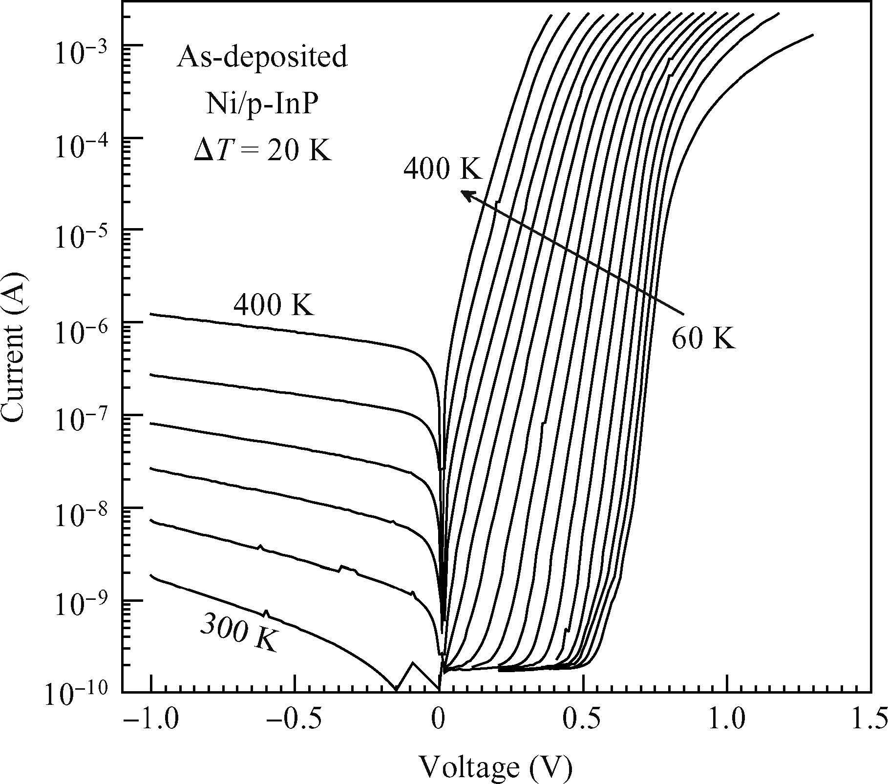
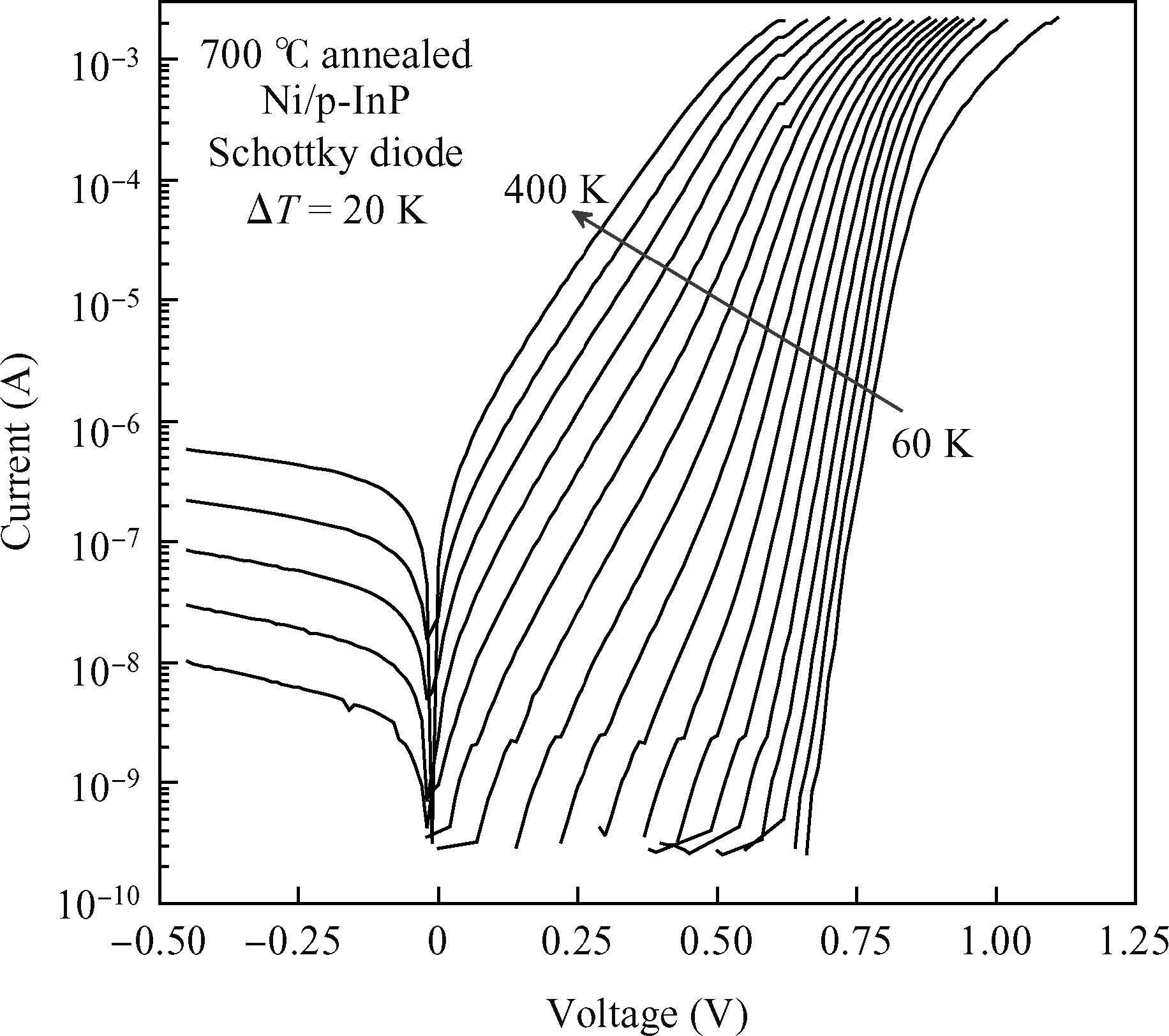
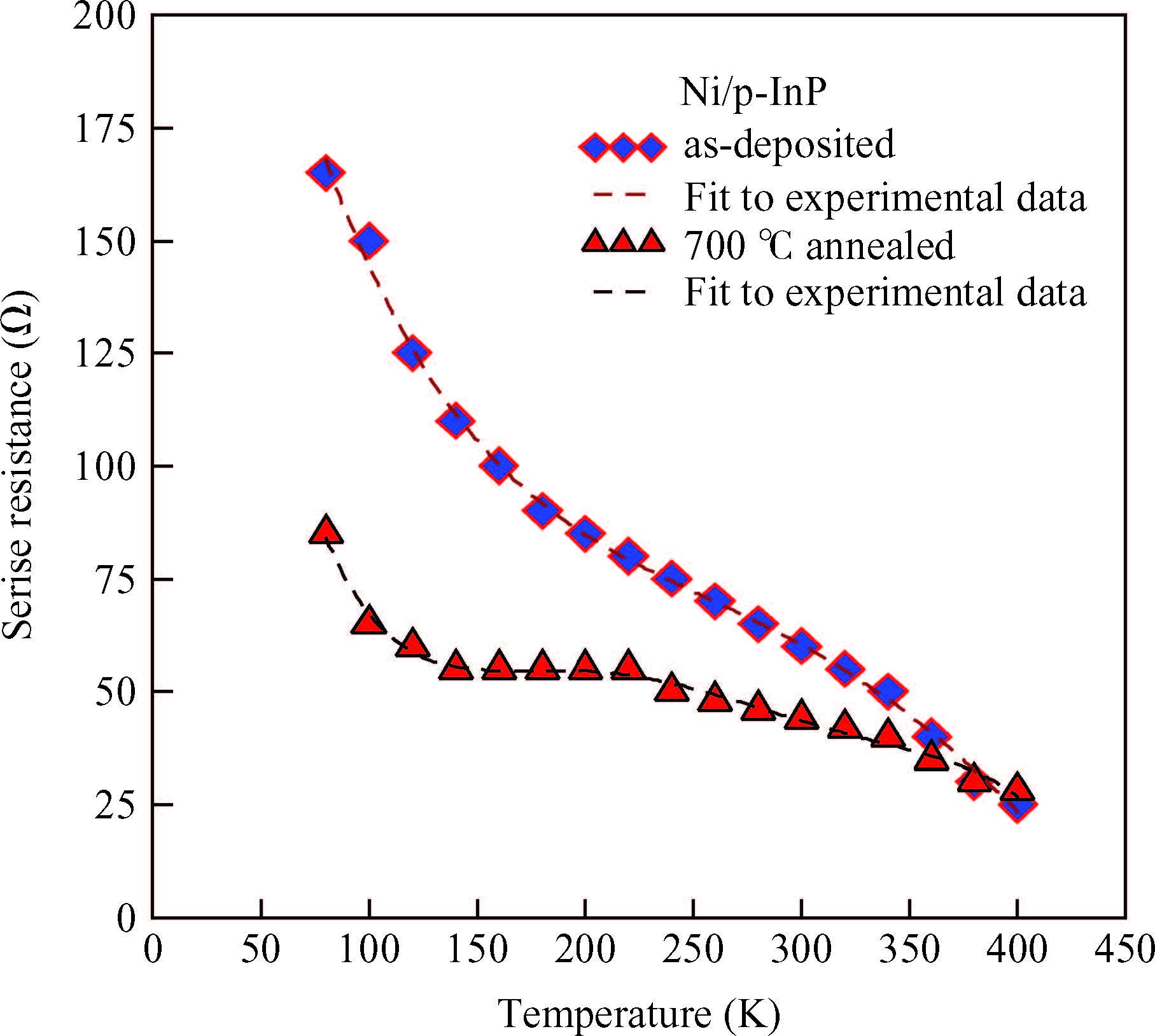
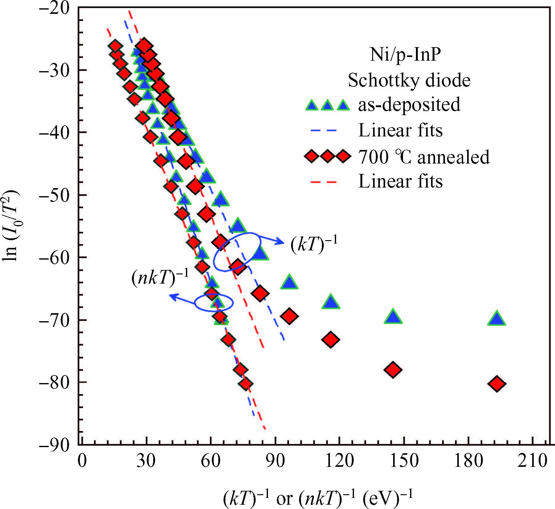
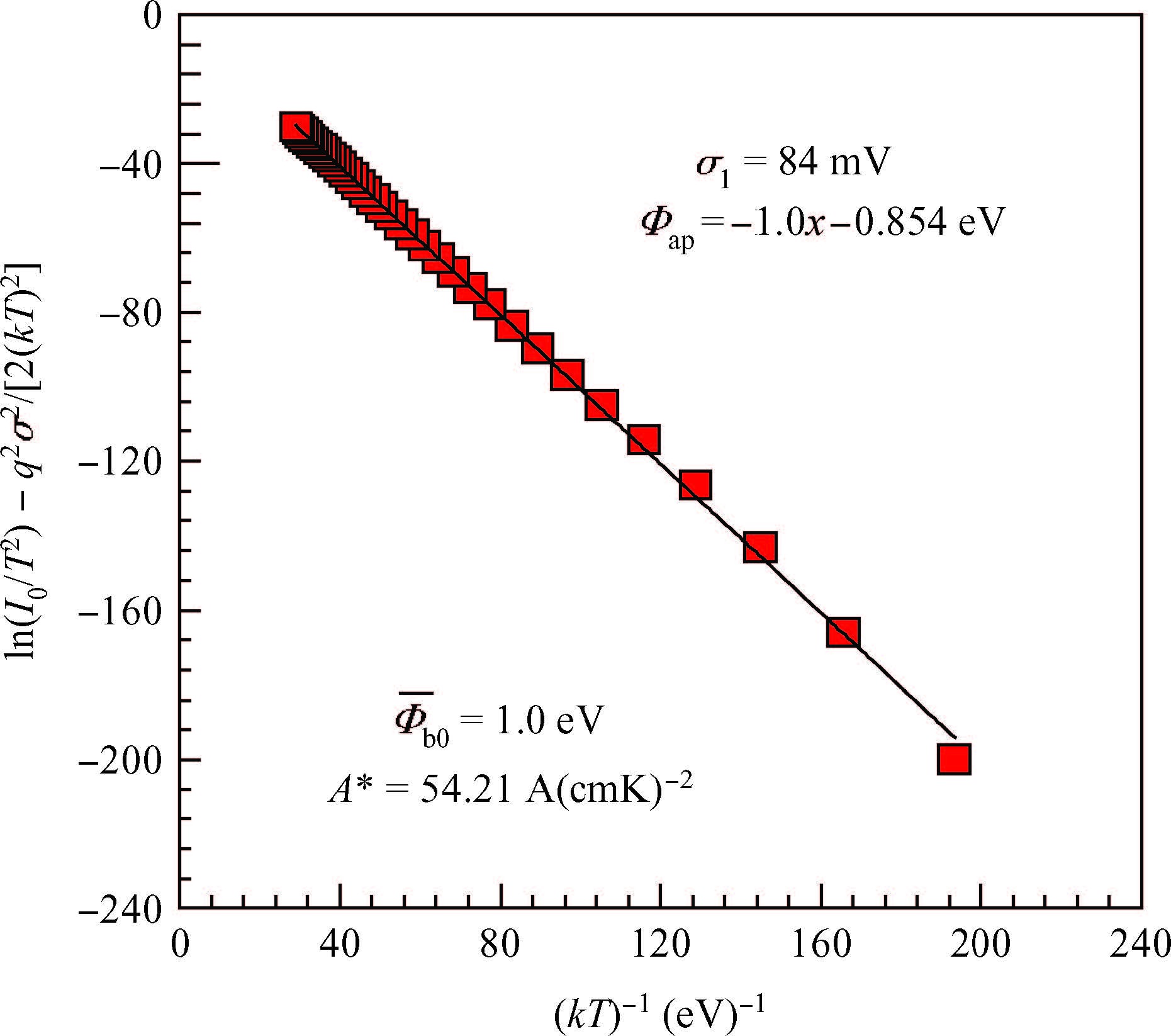
The Ni/p-InP Schottky diodes (SDs) have been prepared by DC magnetron sputtering deposition. After the diode fabrication, they have been thermally annealed at 700℃ for 1 min in N2 atmosphere. Then, the current-voltage characteristics of the annealed and non-annealed (as-deposited) SDs have been measured in the measurement temperature range of 60-400 K with steps of 20 K under dark conditions. After 700℃ annealing, an improvement in the ideality factor value has been observed from 60 to 200 K and the barrier height (BH) value approximately has remained unchanged in the measurement temperature range of 200-400 K. The BH of the annealed diode has decreased obeying the double-Gaussian distribution (GD) of the BHs with decreasing measurement temperature from 200 to 60 K. The BH for the as-deposited diode has decreased with decreasing temperature obeying the single-GD over the whole measurement temperature range. An effective Richardson constant value of 54.21 A/cm2K2 for the as-deposited SD has been obtained from the modified Richardson plot by the single-GD plot, which is in very close agreement with the value of 60 A/K2cm2 for p-type InP. The series resistance value of the annealed SD is lower than that of the non-annealed SD at each temperature and approximately has remained unchanged from 140 to 240 K. Thus, it can be said that an improvement in the diode parameters has been observed due to the thermal annealing at 700℃ for 1 min in N2 atmosphere.


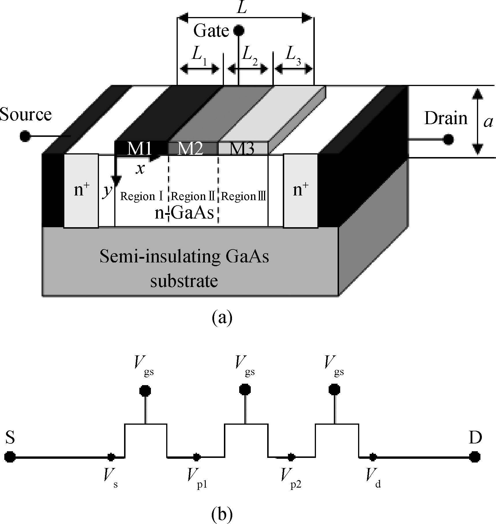
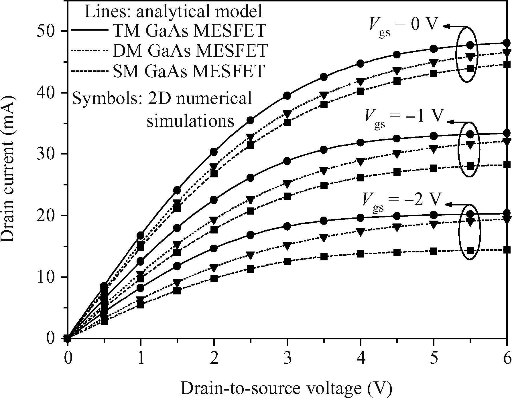
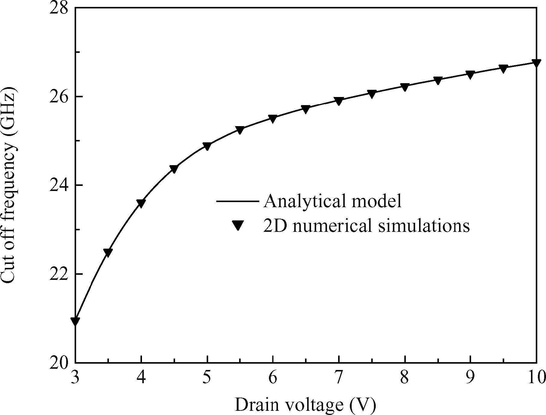
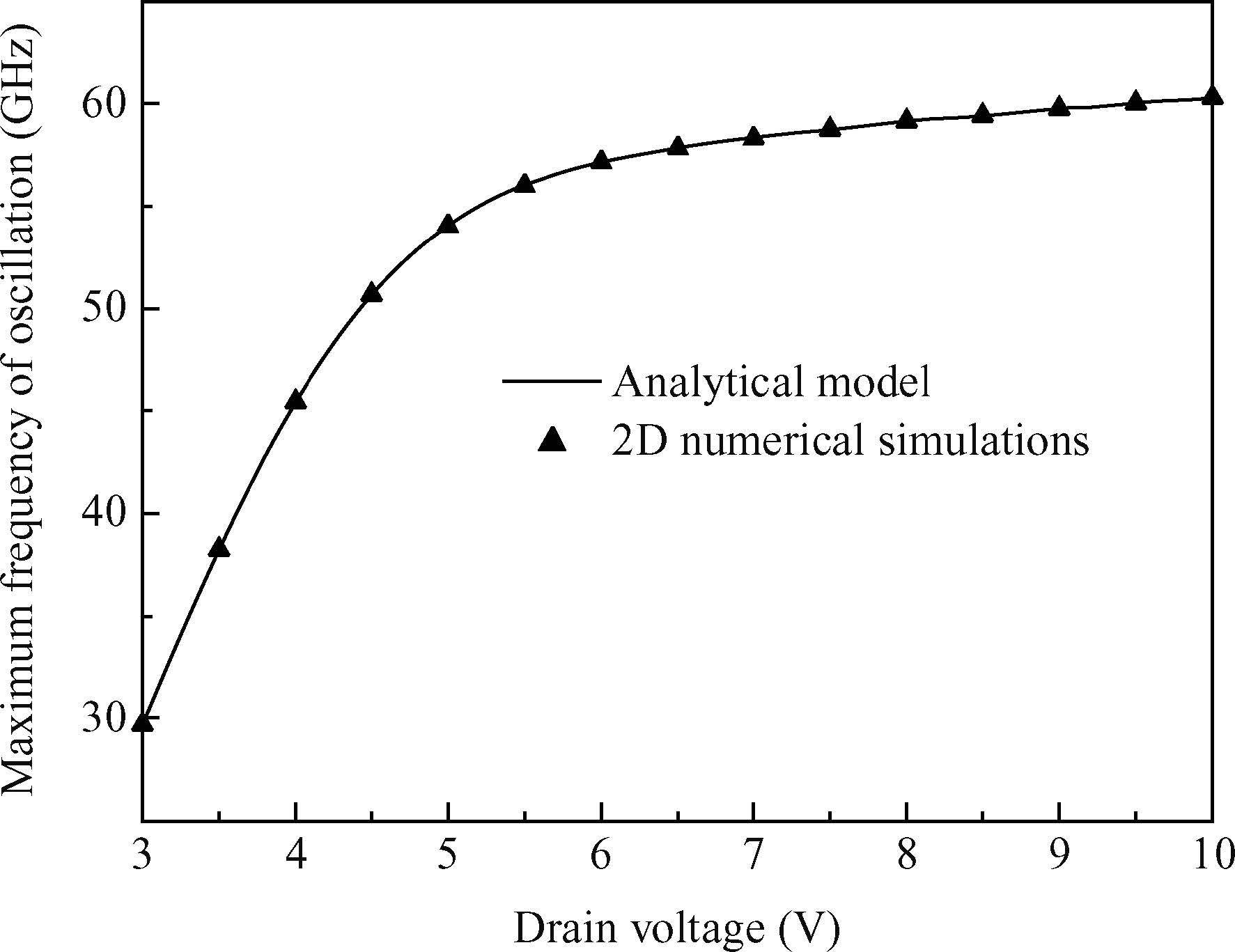
We present an approach of GaAs MESFET incorporating the gate engineering effect to improve immunity against the short channel effects in order to enhance the scaling capability and the device performance for microwave frequency applications. In this context, a physics-based model for I-V characteristics and various microwave characteristics such as transconductance, cut-off frequency and maximum frequency of oscillation of submicron triple material gate (TM) GaAs MESFET are developed. The reduced short channel effects have also been discussed in combined designs i.e. TM, DM and SM in order to show the impact of our approach on the GaAs MESFETs-based device design. The proposed analytical models have been verified by their good agreement with 2D numerical simulations. The models developed in this paper will be useful for submicron and microwave analysis for circuit design.

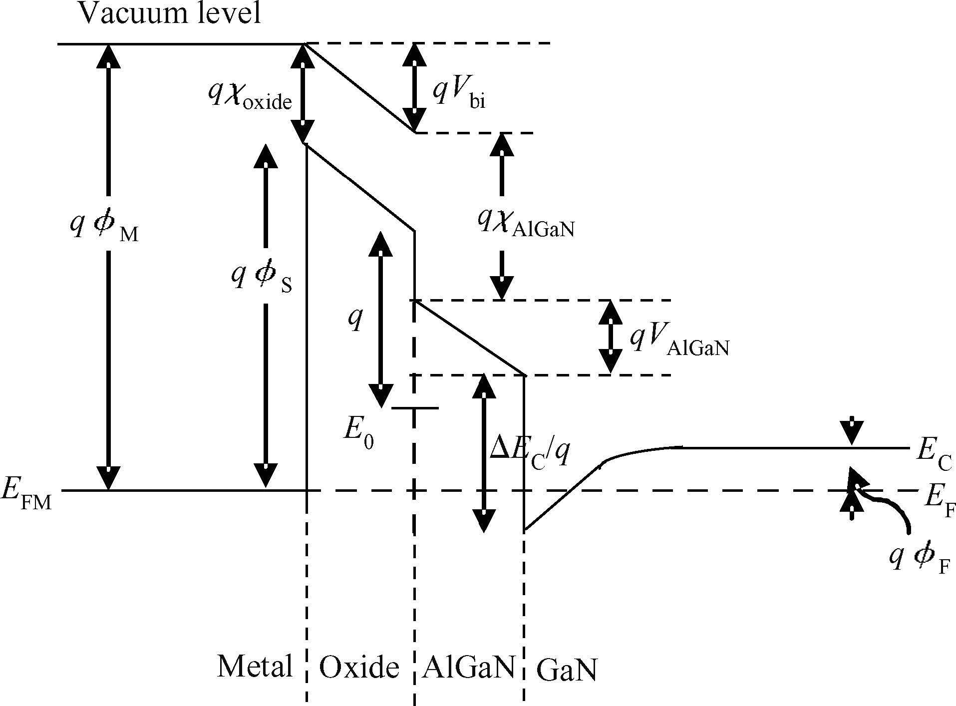
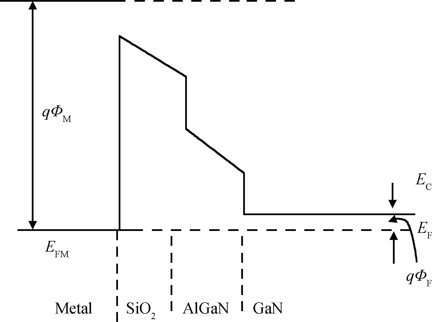
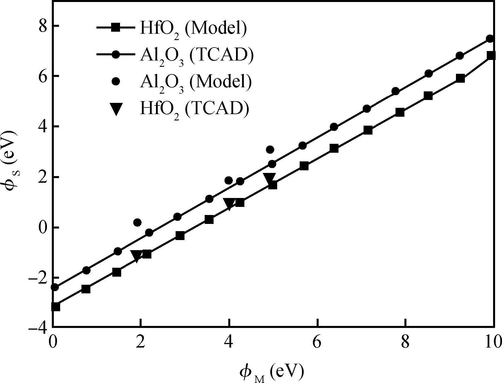
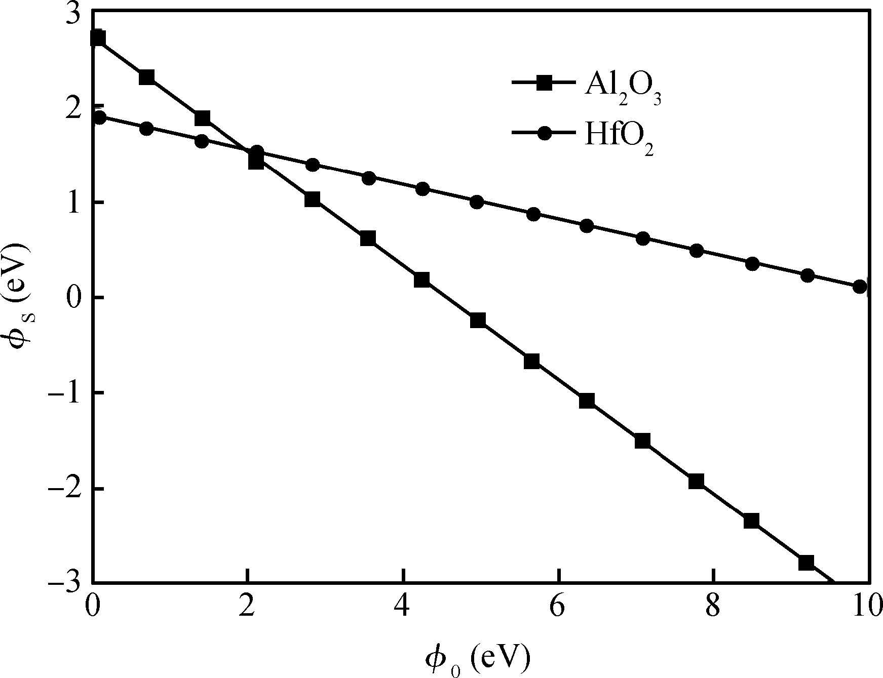
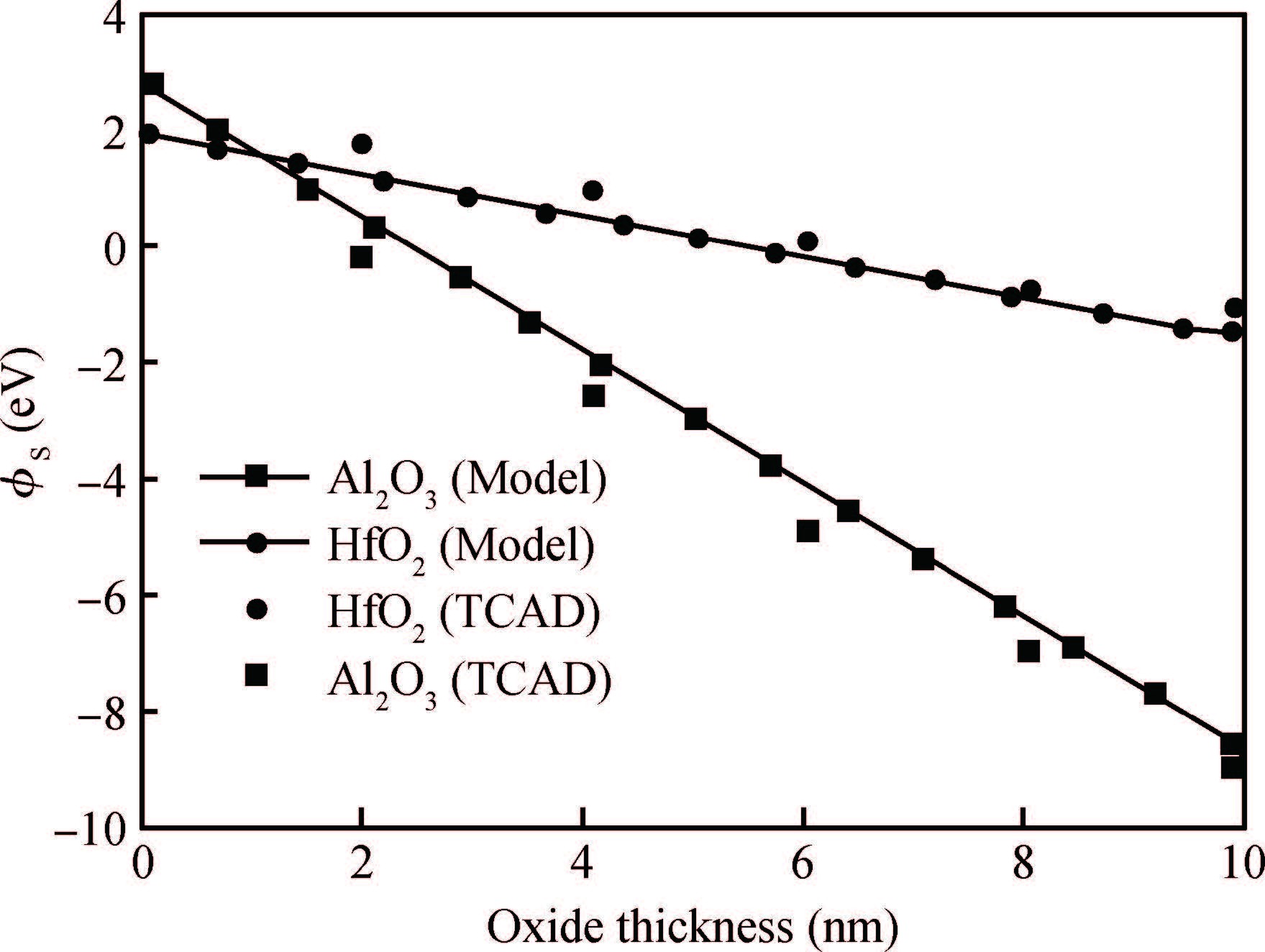
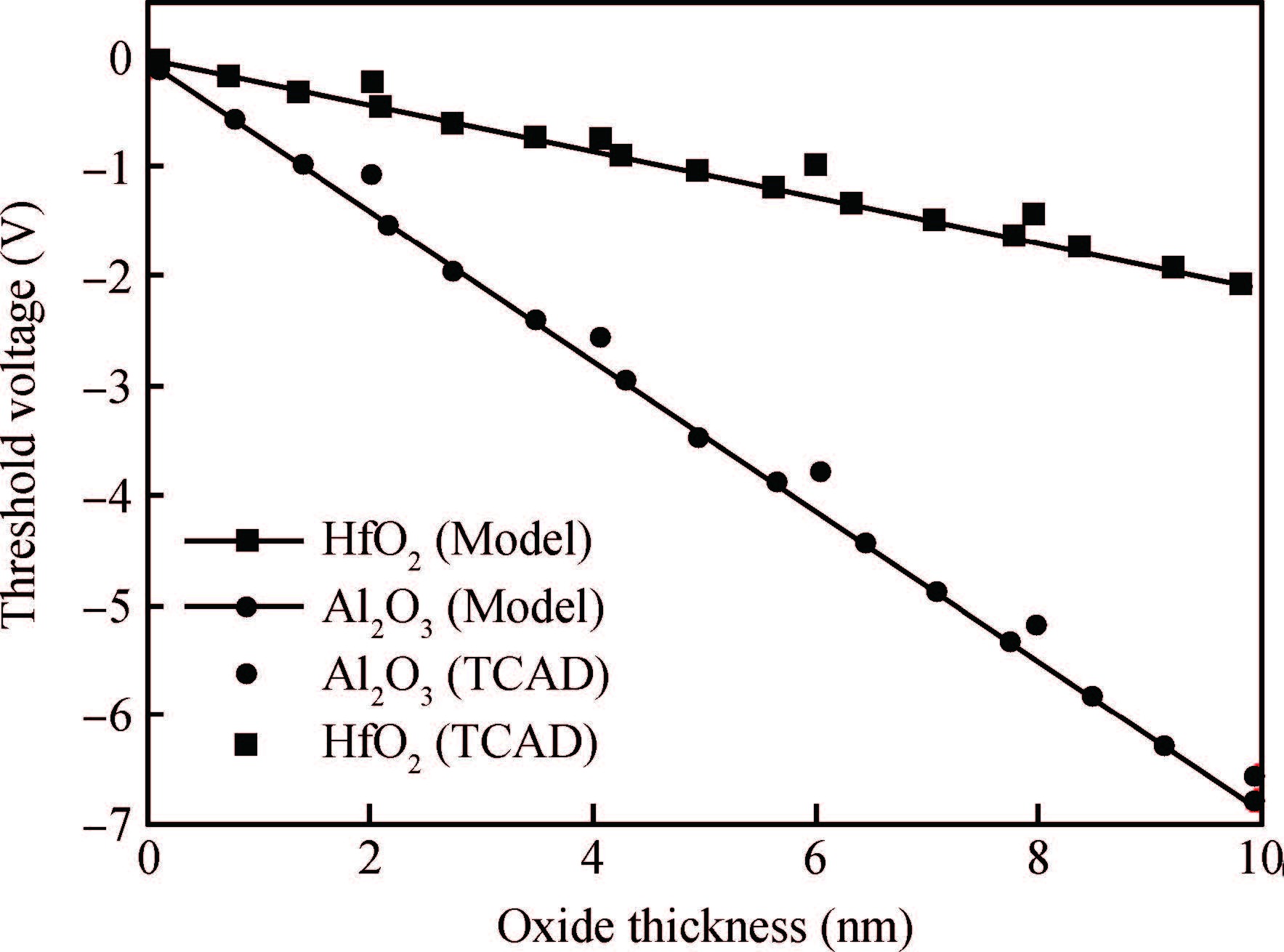
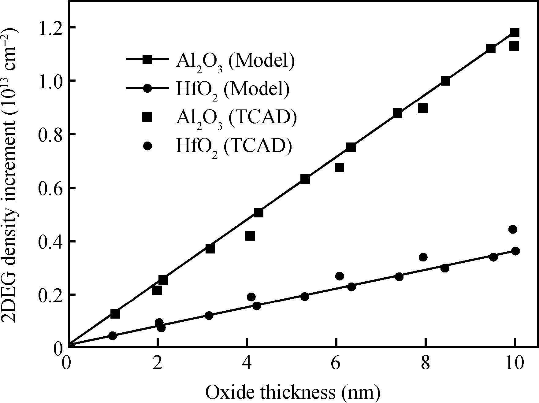
We have developed a physics based analytical model for the calculation of threshold voltage, two dimensional electron gas (2DEG) density and surface potential for AlGaN/GaN metal oxide semiconductor high electron mobility transistors (MOSHEMT). The developed model includes important parameters like polarization charge density at oxide/AlGaN and AlGaN/GaN interfaces, interfacial defect oxide charges and donor charges at the surface of the AlGaN barrier. The effects of two different gate oxides (Al2O3 and HfO2) are compared for the performance evaluation of the proposed MOSHEMT. The MOSHEMTs with Al2O3 dielectric have an advantage of significant increase in 2DEG up to 1.2×1013 cm-2 with an increase in oxide thickness up to 10 nm as compared to HfO2 dielectric MOSHEMT. The surface potential for HfO2 based device decreases from 2 to -1.6 eV within 10 nm of oxide thickness whereas for the Al2O3 based device a sharp transition of surface potential occurs from 2.8 to -8.3 eV. The variation in oxide thickness and gate metal work function of the proposed MOSHEMT shifts the threshold voltage from negative to positive realizing the enhanced mode operation. Further to validate the model, the device is simulated in Silvaco Technology Computer Aided Design (TCAD) showing good agreement with the proposed model results. The accuracy of the developed calculations of the proposed model can be used to develop a complete physics based 2DEG sheet charge density and threshold voltage model for GaN MOSHEMT devices for performance analysis.

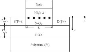
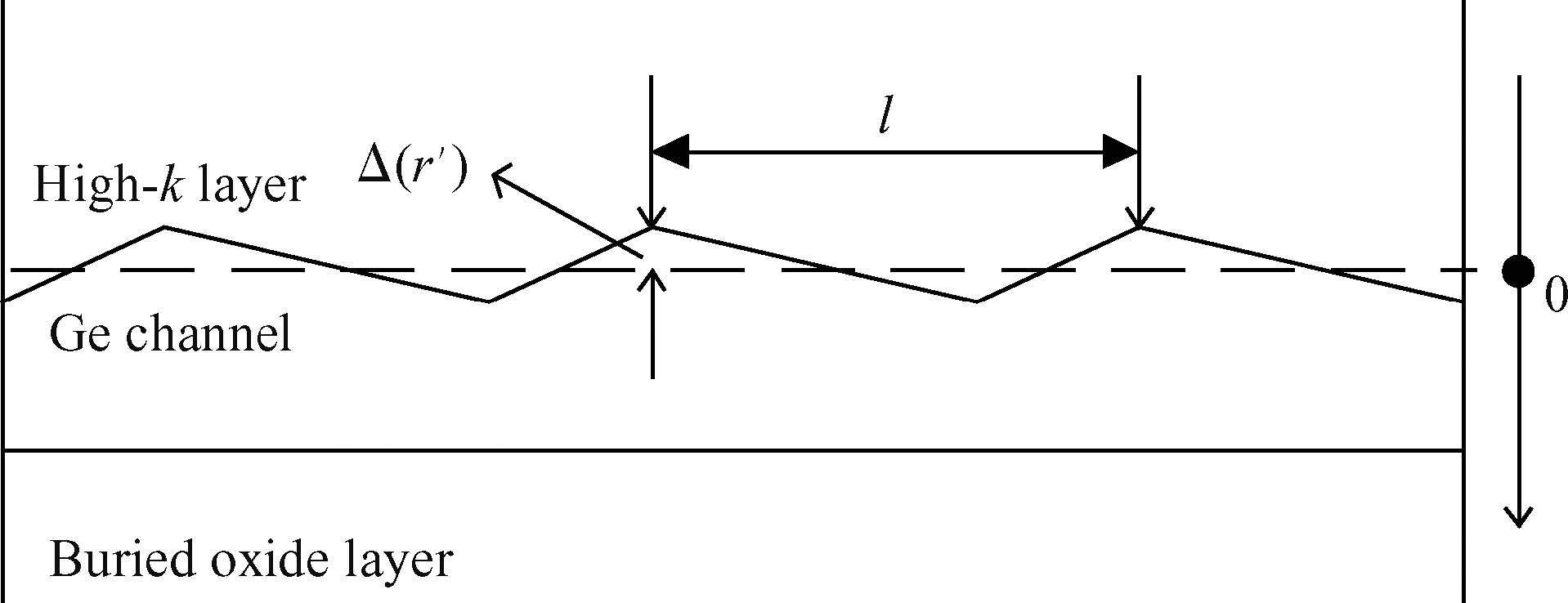
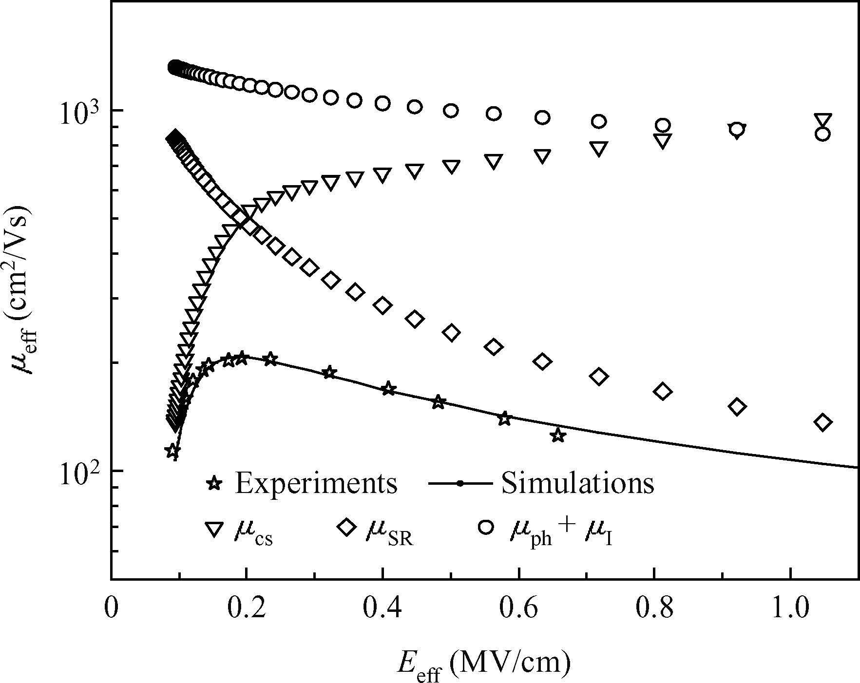
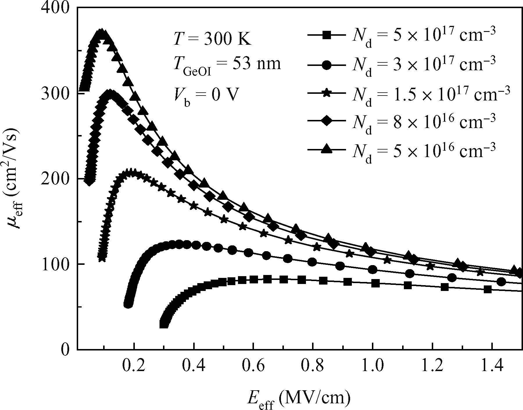
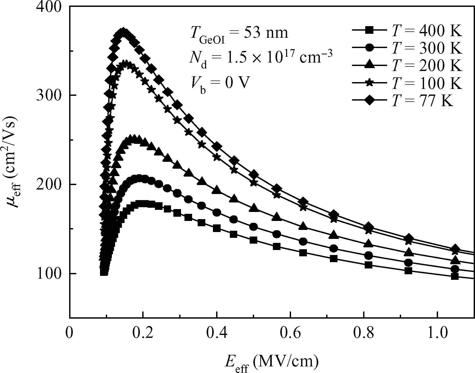
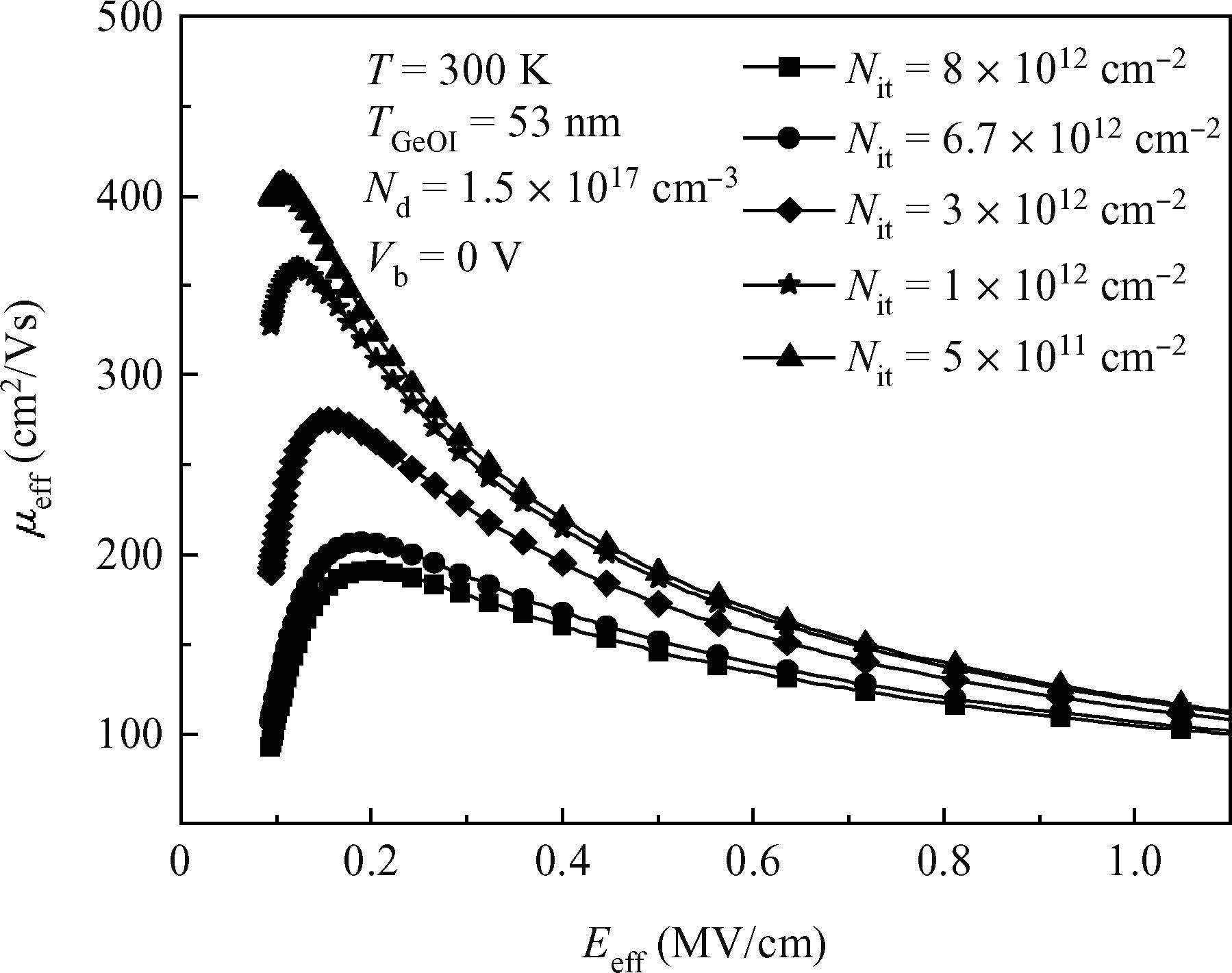
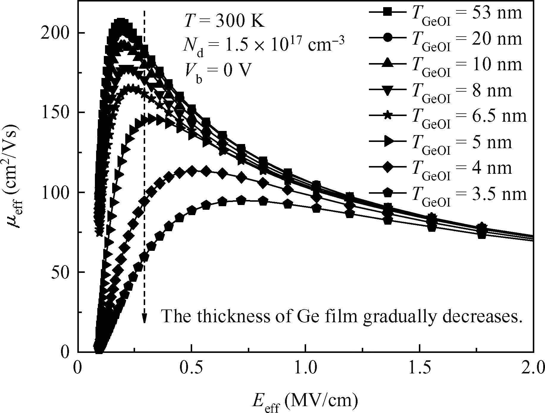
A physical model of hole mobility for germanium-on-insulator pMOSFETs is built by analyzing all kinds of scattering mechanisms, and a good agreement of the simulated results with the experimental data is achieved, confirming the validity of this model. The scattering mechanisms involved in this model include acoustic phonon scattering, ionized impurity scattering, surface roughness scattering, coulomb scattering and the scattering caused by Ge film thickness fluctuation. The simulated results show that the coulomb scattering from the interface charges is responsible for the hole mobility degradation in the low-field regime and the surface roughness scattering limits the hole mobility in the high-field regime. In addition, the effects of some factors, e.g. temperature, doping concentration of the channel and the thickness of Ge film, on degradation of the mobility are also discussed using the model, thus obtaining a reasonable range of the relevant parameters.


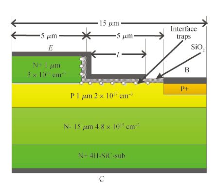
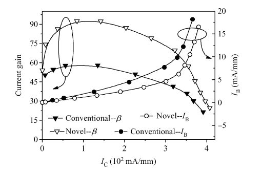
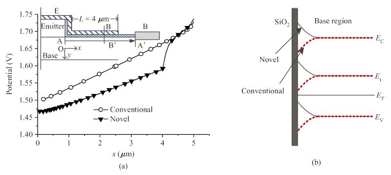
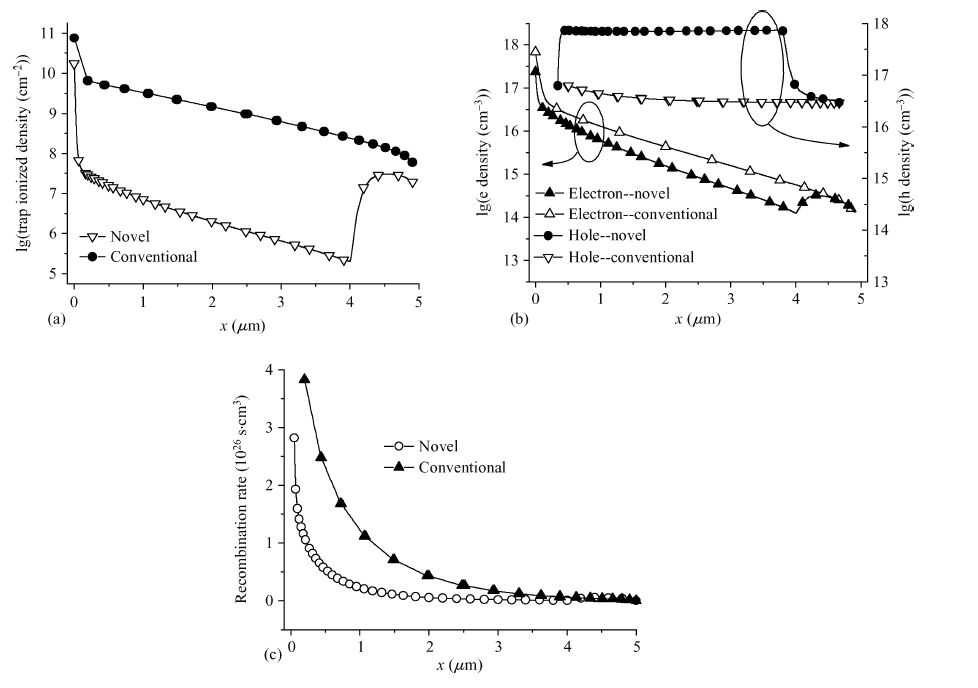
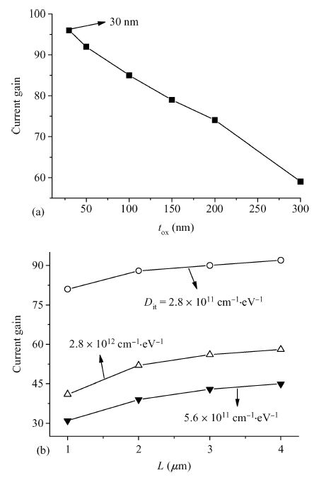
A novel 4H-SiC BJT of high current gain with a suppressing surface traps effect has been proposed. It is effective to improve the current gain due to the lower electrons density in the surface region by extending the emitter metal to overlap the passivation layer on the extrinsic base surface. The electrons trapped in the extrinsic base surface induce the degeneration of SiC BJTs device performance. By modulating the electron recombination rate, the novel structure can increase the current gain to 63.2% compared with conventional ones with the compatible process technology. Optimized sizes are an overlapped metal length of 4 μm, as well as an oxide layer thickness of 50 nm.

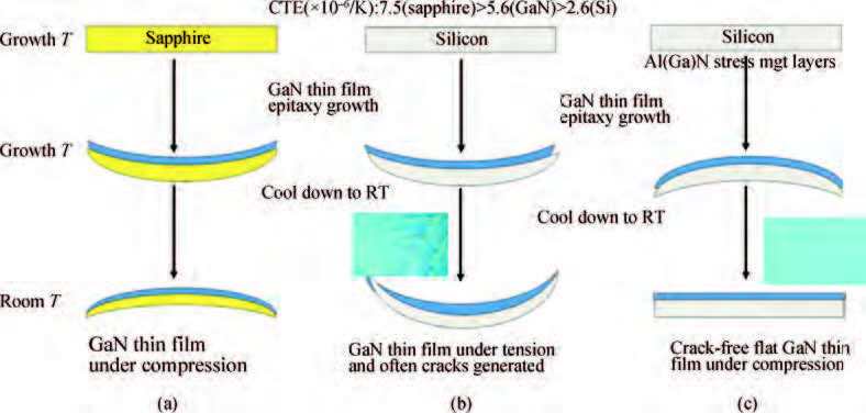
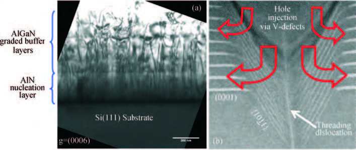
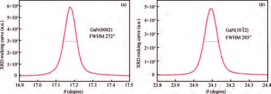
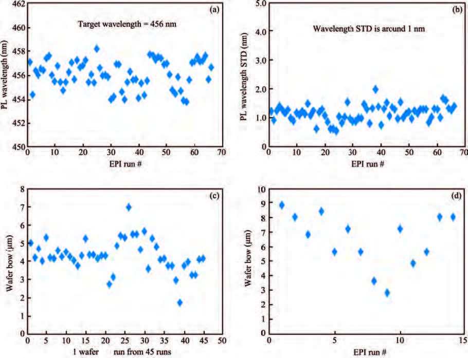
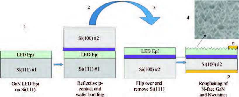
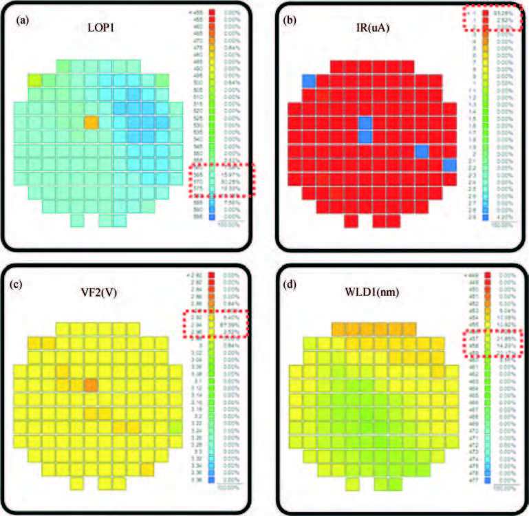
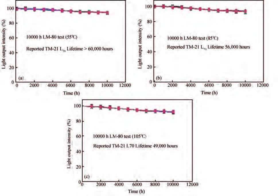
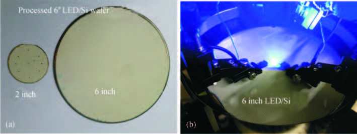
The dream of epitaxially integrating Ⅲ-nitride semiconductors on large diameter silicon is being fulfilled through the joint R&D efforts of academia and industry, which is driven by the great potential of GaN-on-silicon technology in improving the efficiency yet at a much reduced manufacturing cost for solid state lighting and power electronics. It is very challenging to grow high quality GaN on Si substrates because of the huge mismatch in the coefficient of thermal expansion (CTE) and the large mismatch in lattice constant between GaN and silicon, often causing a micro-crack network and a high density of threading dislocations (TDs) in the GaN film. Al-composition graded AlGaN/AlN buffer layers have been utilized to not only build up a compressive strain during the high temperature growth for compensating the tensile stress generated during the cool down, but also filter out the TDs to achieve crack-free high-quality n-GaN film on Si substrates, with an X-ray rocking curve linewidth below 300 arcsec for both (0002) and (1012) diffractions. Upon the GaN-on-Si templates, prior to the deposition of p-AlGaN and p-GaN layers, high quality InGaN/GaN multiple quantum wells (MQWs) are overgrown with well-engineered V-defects intentionally incorporated to shield the TDs as non-radiative recombination centers and to enhance the hole injection into the MQWs through the via-like structures. The as-grown GaN-on-Si LED wafers are processed into vertical structure thin film LED chips with a reflective p-electrode and the N-face surface roughened after the removal of the epitaxial Si(111) substrates, to enhance the light extraction efficiency. We have commercialized GaN-on-Si LEDs with an average efficacy of 150-160 lm/W for 1 mm2 LED chips at an injection current of 350 mA, which have passed the 10000-h LM80 reliability test. The as-produced GaN-on-Si LEDs featured with a single-side uniform emission and a nearly Lambertian distribution can adopt the wafer-level phosphor coating procedure, and are suitable for directional lighting, camera flash, streetlighting, automotive headlamps, and otherlighting applications.


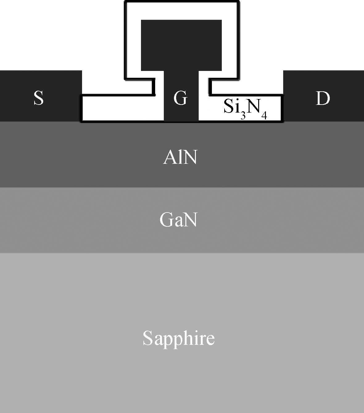
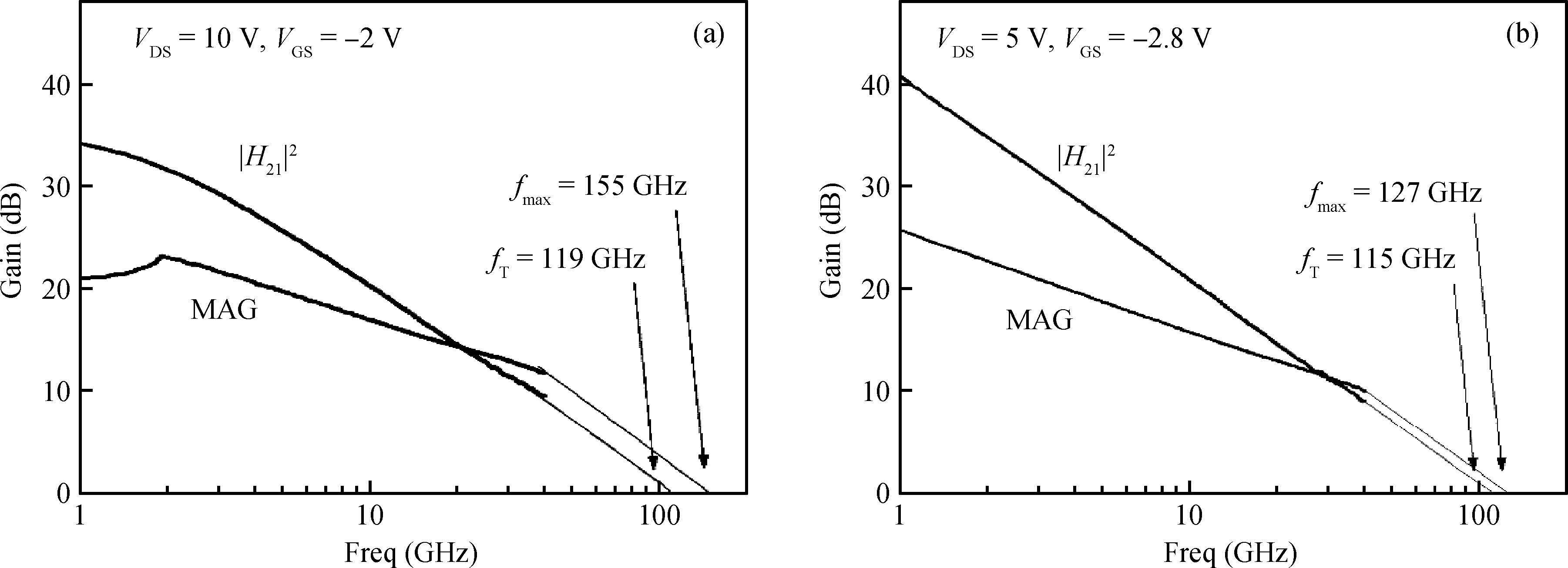
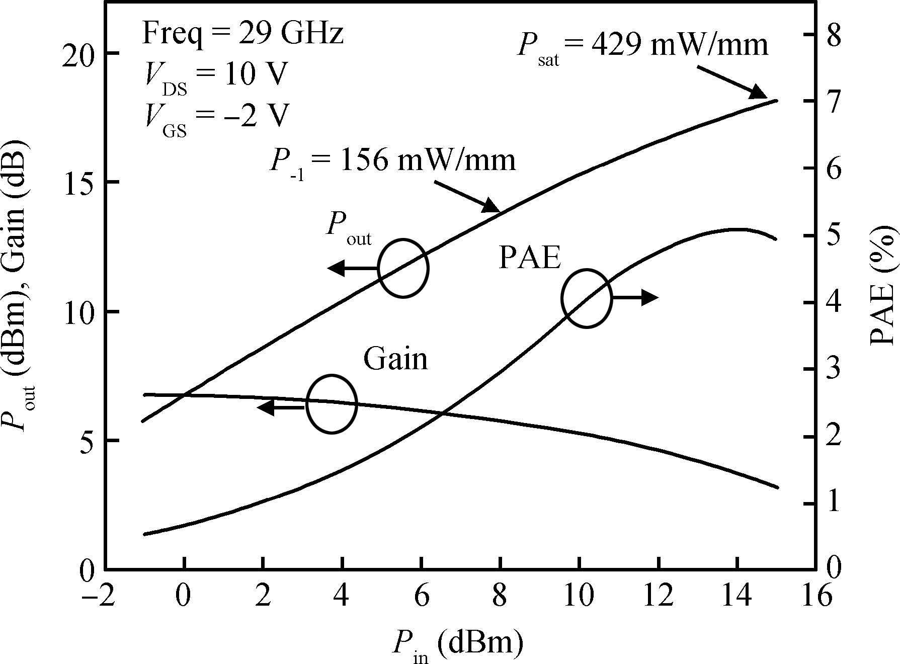
We report the DC and RF characteristics of AlN/GaN high electron mobility transistors (HEMTs) with the gate length of 100 nm on sapphire substrates. The device exhibits a maximum drain current density of 1.29 A/mm and a peak transconductance of 440 mS/mm. A current gain cutoff frequency and a maximum oscillation frequency of 119 GHz and 155 GHz have been obtained, respectively. Furthermore, the large signal load pull characteristics of the AlN/GaN HEMTs were measured at 29 GHz. An output power density of 429 mW/mm has been demonstrated at a drain bias of 10 V. To the authors' best knowledge, this is the earliest demonstration of power density at the Ka band for AlN/GaN HEMTs in the domestic, and also a high frequency of load-pull measurements for AlN/GaN HEMTs.


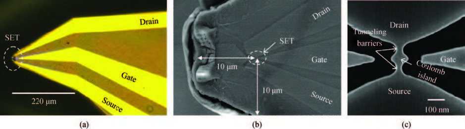
Single electron transistors (SETs) are known to be extremely sensitive electrometers owing to their high charge sensitivity. In this work, we report the design, fabrication, and characterization of a silicon-on-insulator-based SET scanning probe. The fabricated SET is located about 10 μm away from the probe tip. The SET with a quantum dot of about 70 nm in diameter exhibits an obvious Coulomb blockade effect measured at 4.1 K. The Coulomb blockade energy is about 18 meV, and the charge sensitivity is in the order of 10-5-10-3 e/Hz1/2. This SET scanning probe can be used to map charge distribution and sense dynamic charge fluctuation in nanodevices or circuits under test, realizing high sensitivity and high spatial resolution charge detection.

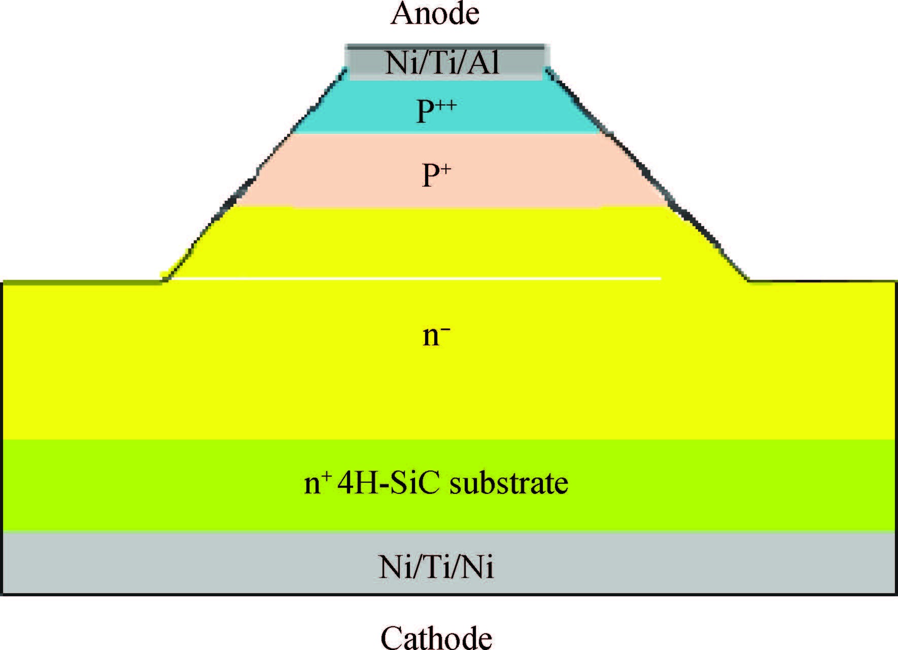
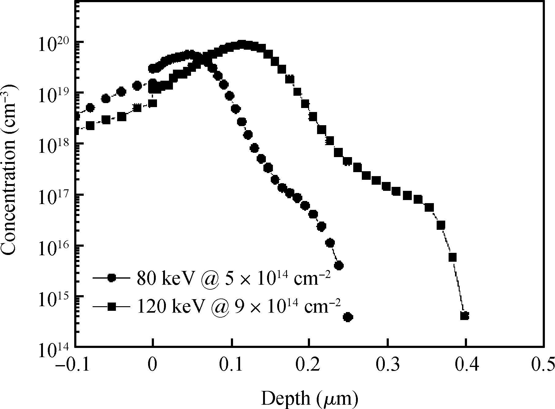
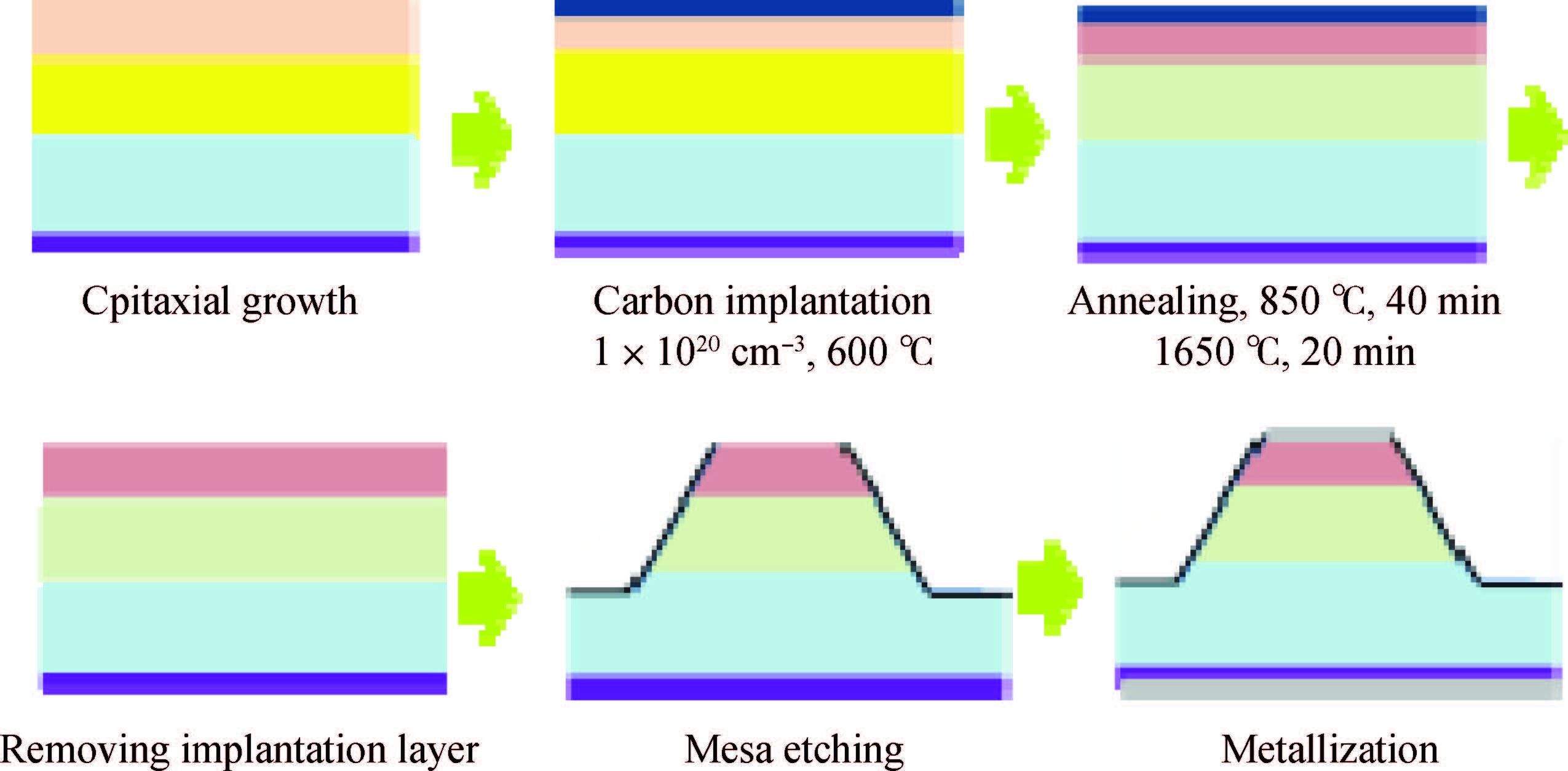
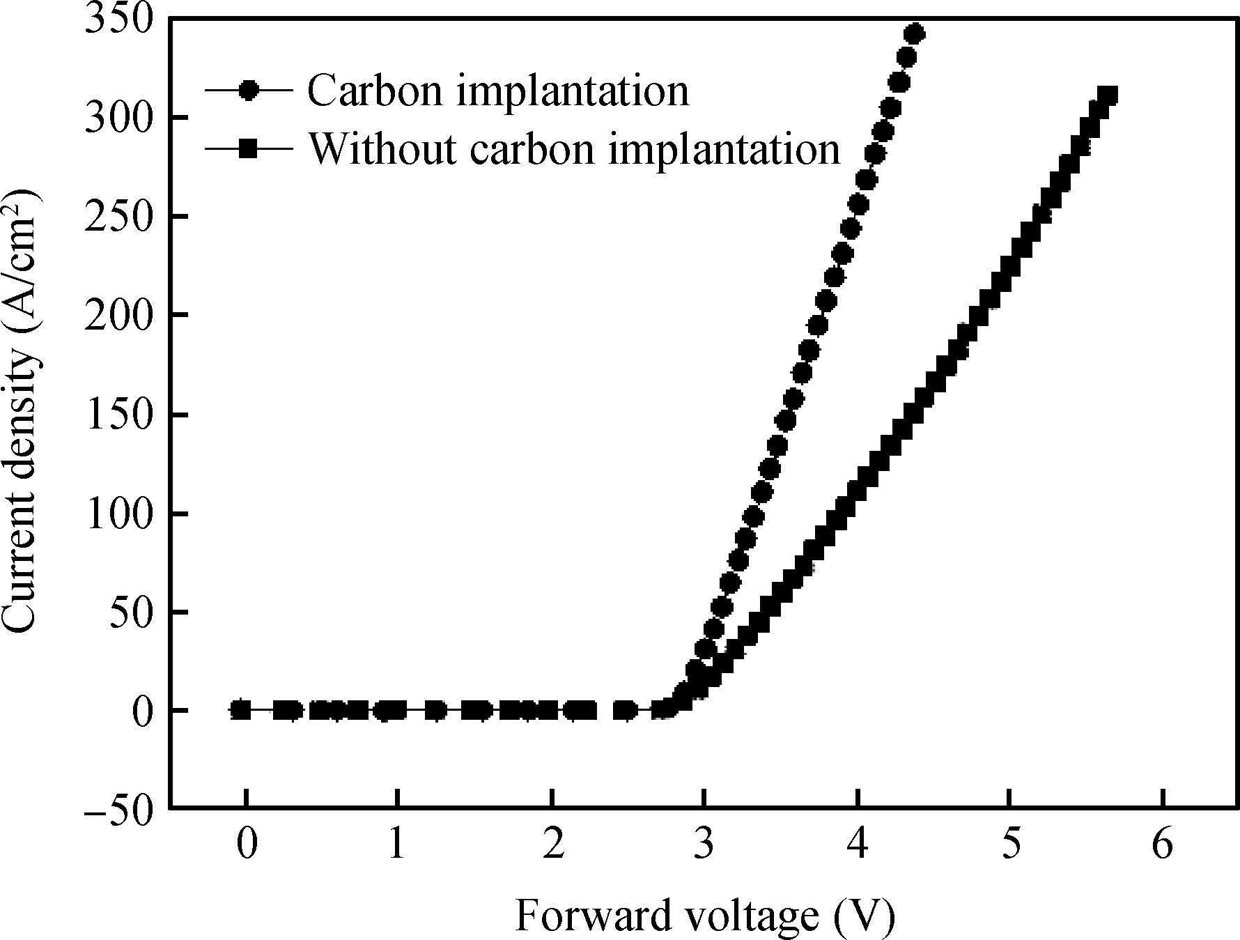
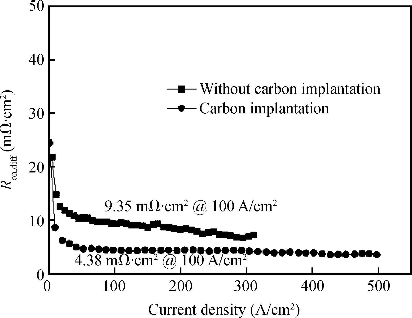
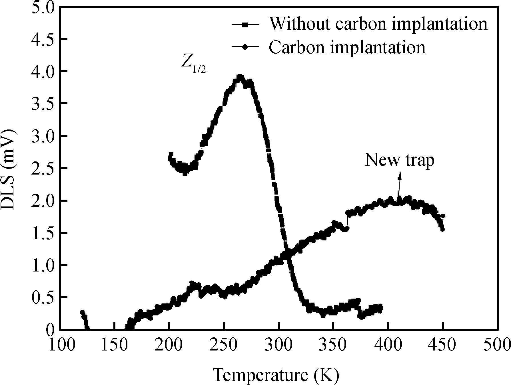
The characteristics of 4H-SiC PiN diodes with a carbon-implanted drift layer was investigated and the reason of characteristics improvement was analyzed. The forward voltage drops of the diodes with carbon-implanted drift layer were around 3.3 V, which is lower than that of devices without carbon implantation, the specific-on resistance was decreased from 9.35 to 4.38 mΩ·cm2 at 100 A/cm2, and the reverse leakage current was also decreased. The influence of carbon incorporation in the SiC crystalline grids was studied by using deep-level transient spectroscopy (DLTS). The DLTS spectra revealed that the Z1/2 traps, which were regarded as the main lifetime limiting defects, were dramatically reduced. It is proposed that the reduction of Z1/2 traps can achieve longer carrier lifetime in the drift layer, which is beneficial to the performance of bipolar devices.


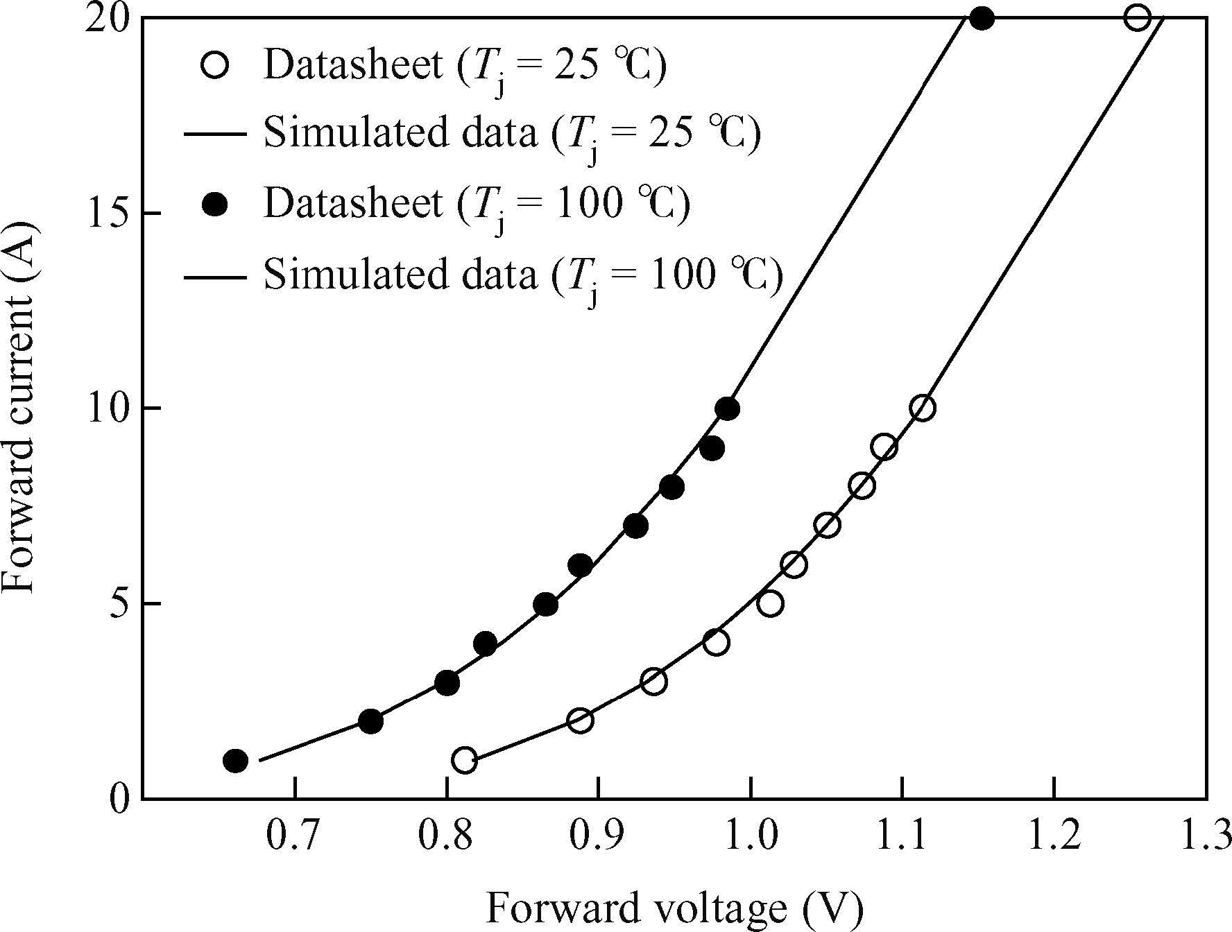
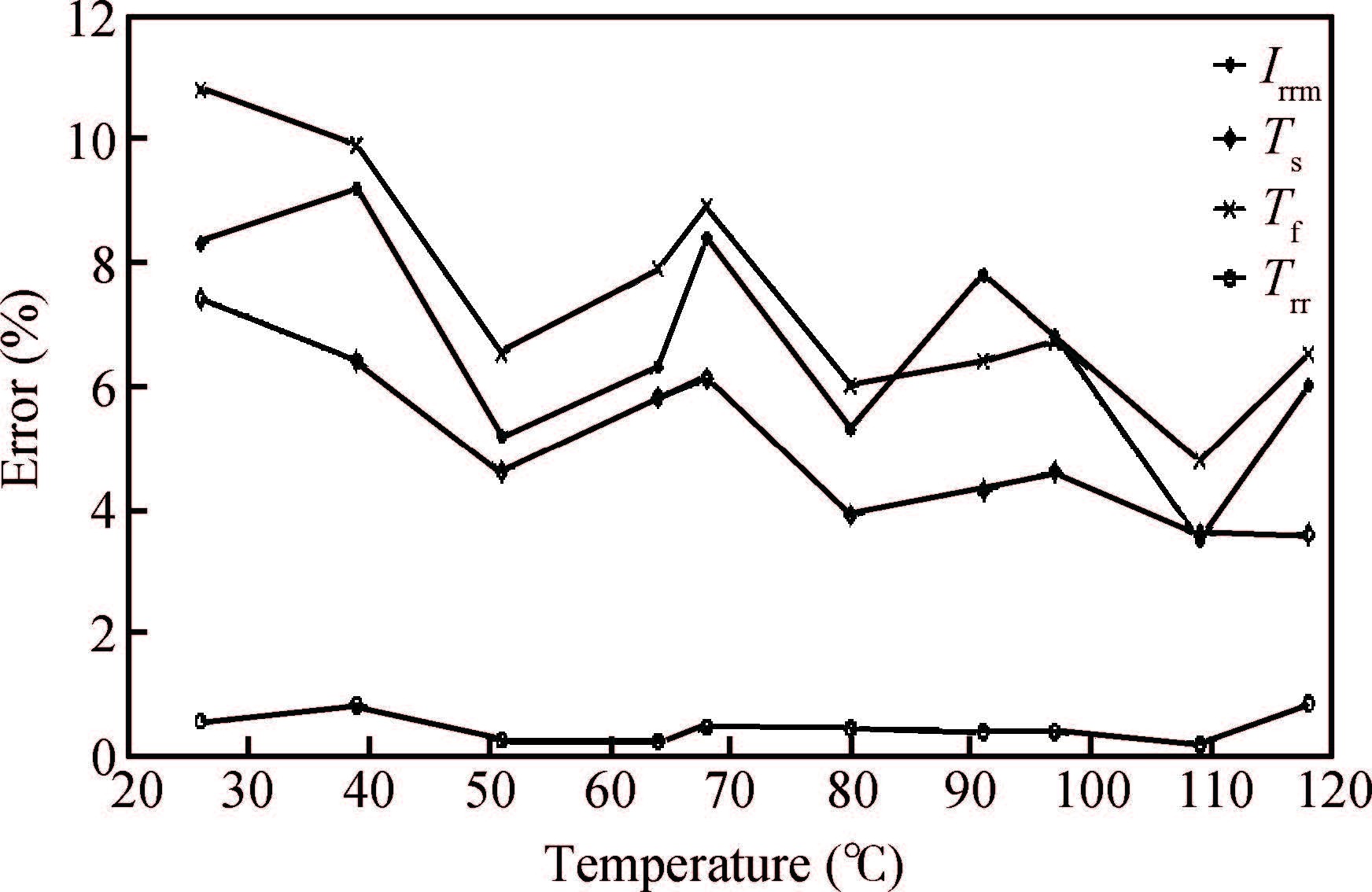
The PIN diode model for high frequency dynamic transient characteristic simulation is important in conducted EMI analysis. The model should take junction temperature into consideration since equipment usually works at a wide range of temperature. In this paper, a temperature-variable high frequency dynamic model for the PIN diode is built, which is based on the Laplace-transform analytical model at constant temperature. The relationship between model parameters and temperature is expressed as temperature functions by analyzing the physical principle of these parameters. A fast recovery power diode MUR1560 is chosen as the test sample and its dynamic performance is tested under inductive load by a temperature chamber experiment, which is used for model parameter extraction and model verification. Results show that the model proposed in this paper is accurate for reverse recovery simulation with relatively small errors at the temperature range from 25 to 120℃.


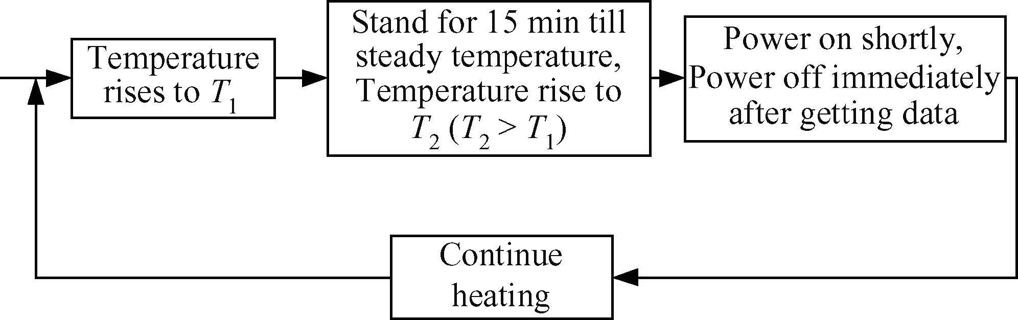
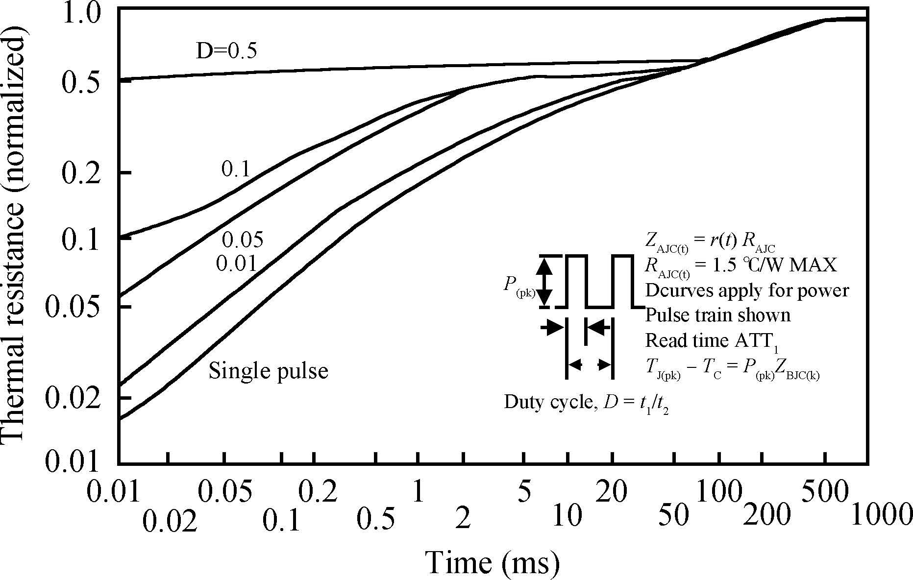
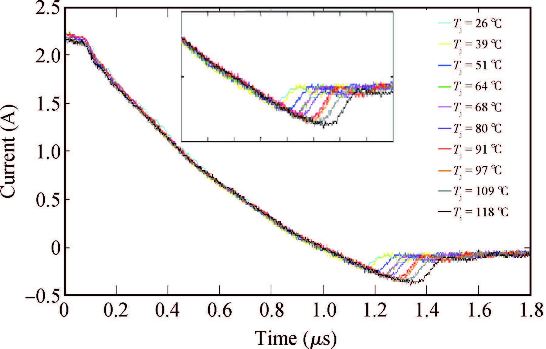
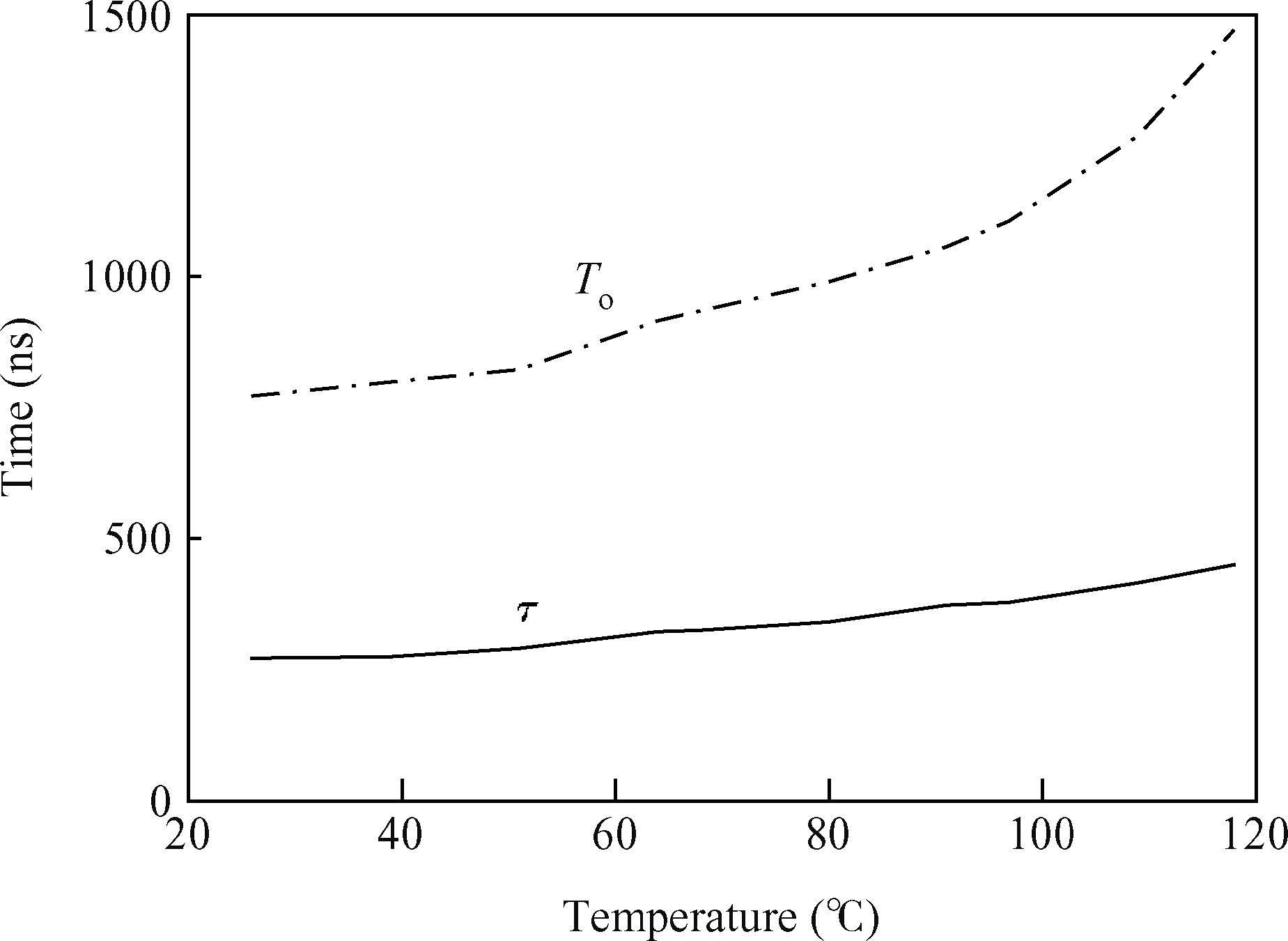

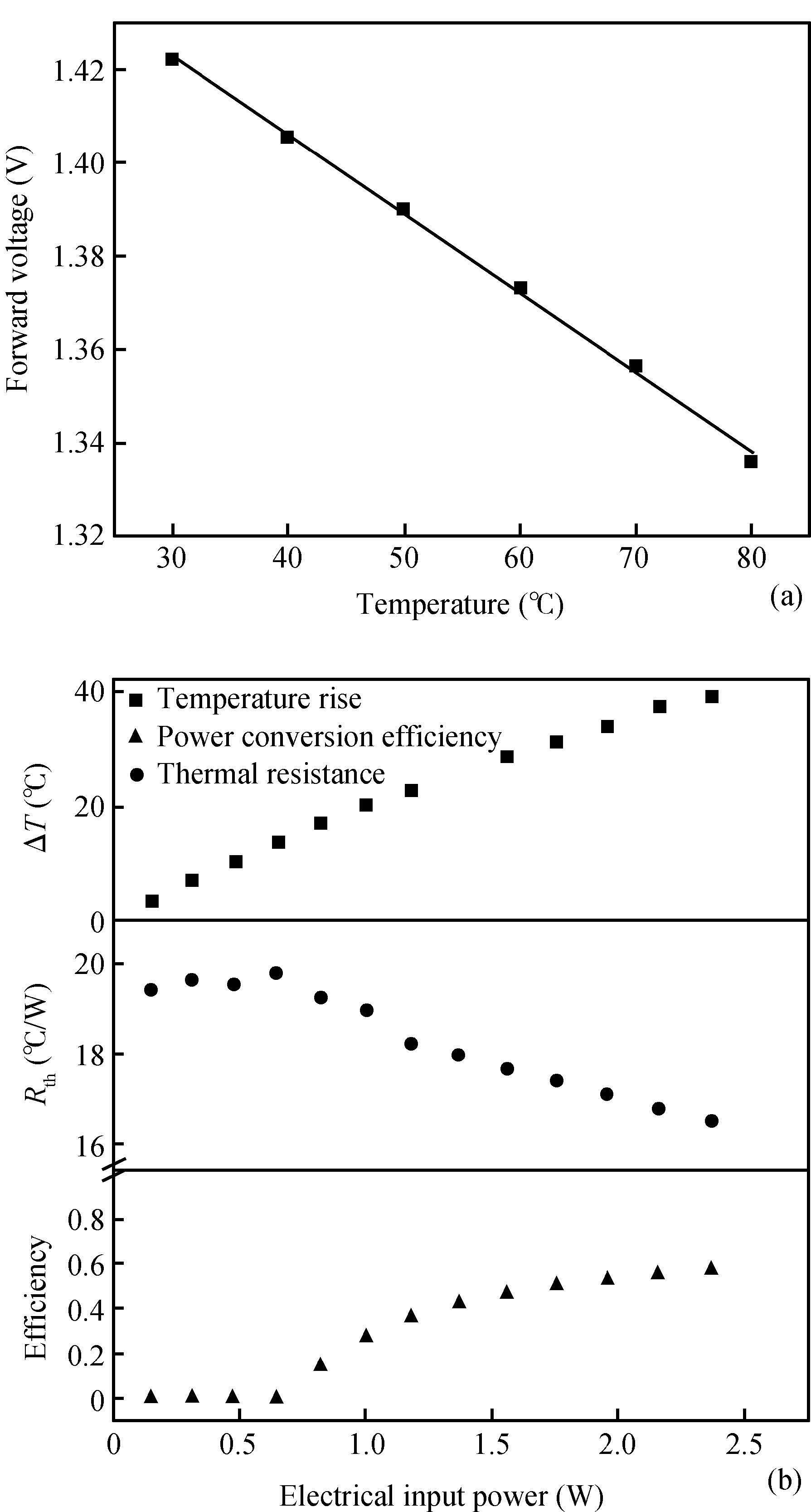
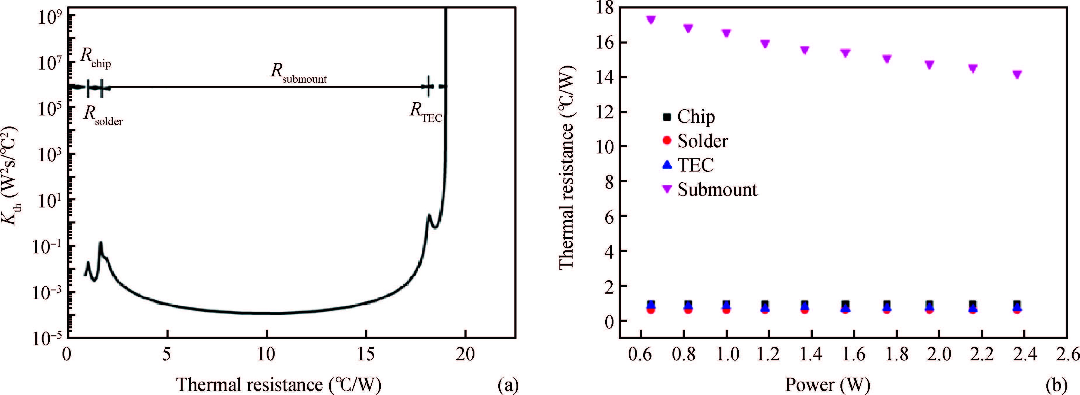
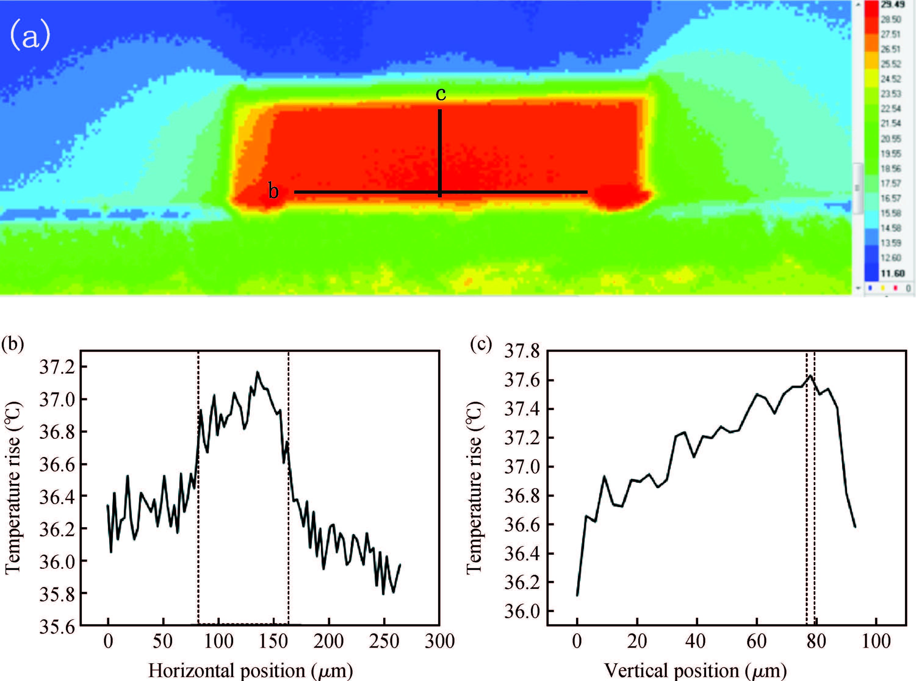
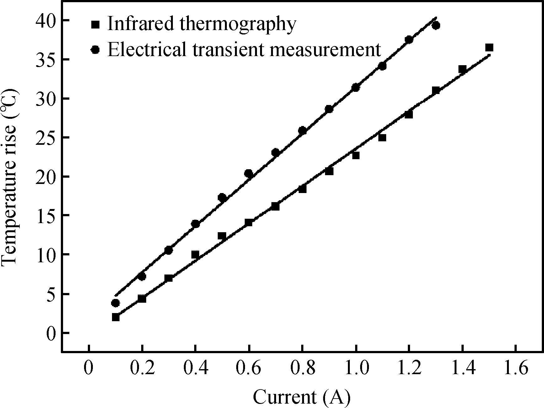
The thermal characteristics of 808 nm AlGaAs/GaAs laser diodes (LDs) are analyzed via electrical transient measurements and infrared thermography. The temperature rise and thermal resistance are measured at various input currents and powers. From the electrical transient measurements, it is found that there is a significant reduction in thermal resistance with increasing power because of the device power conversion efficiency. The component thermal resistance that was obtained from the structure function showed that the total thermal resistance is mainly composed of the thermal resistance of the sub-mount rather than that of the LD chip, and the thermal resistance of the sub-mount decreases with increasing current. The temperature rise values are also measured by infrared thermography and are calibrated based on a reference image, with results that are lower than those determined by electrical transient measurements. The difference in the results is caused by the limited spatial resolution of the measurements and by the signal being captured from the facet rather than from the junction of the laser diode.

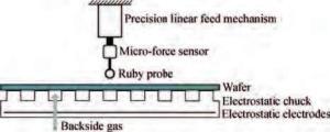
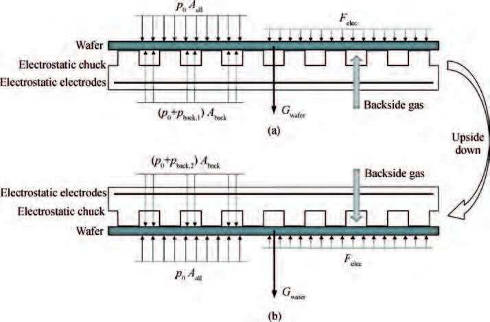
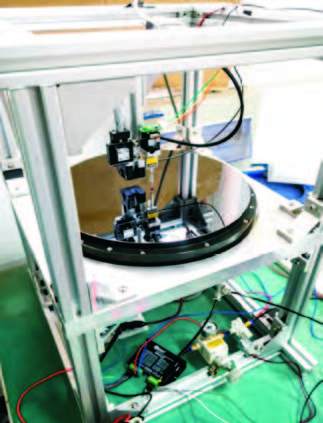
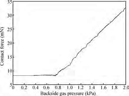
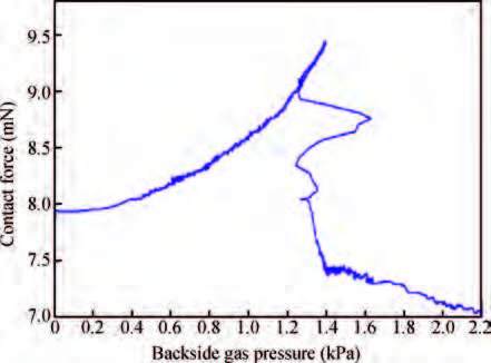
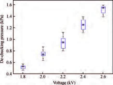
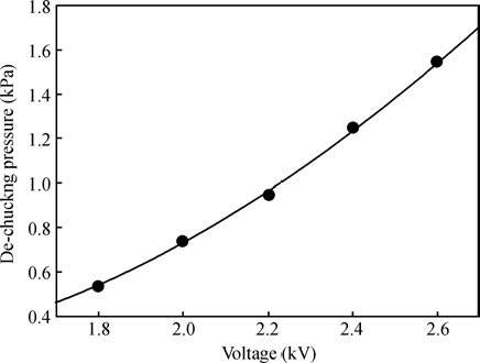
Electrostatic chucks are one of the core components of semiconductor devices. As a key index of electrostatic chucks, the clamping force must be controlled within a reasonable range. Therefore, it is essential to accurately measure the clamping force. To reduce the negative factors influencing measurement precision and repeatability, this article presents a novel method to measure the clamping force and we elaborate both the principle and the key procedure. A micro-force probe component is introduced to monitor, adjust, and eliminate the gap between the wafer and the electrostatic chuck. The contact force between the ruby probe and the wafer is selected as an important parameter to characterize de-chucking, and we have found that the moment of de-chucking can be exactly judged. Moreover, this article derives the formula calibrating equivalent action area of backside gas pressure under real working conditions, which can effectively connect the backside gas pressure at the moment of de-chucking and the clamping force. The experiments were then performed on a self-designed measuring platform. The de-chucking mechanism is discussed in light of our analysis of the experimental data. Determination criteria for de-chucking point are summed up. It is found that the relationship between de-chucking pressure and applied voltage conforms well to quadratic equation. Meanwhile, the result reveals that actual de-chucking behavior is much more complicated than the description given in the classical empirical formula.


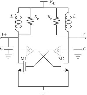
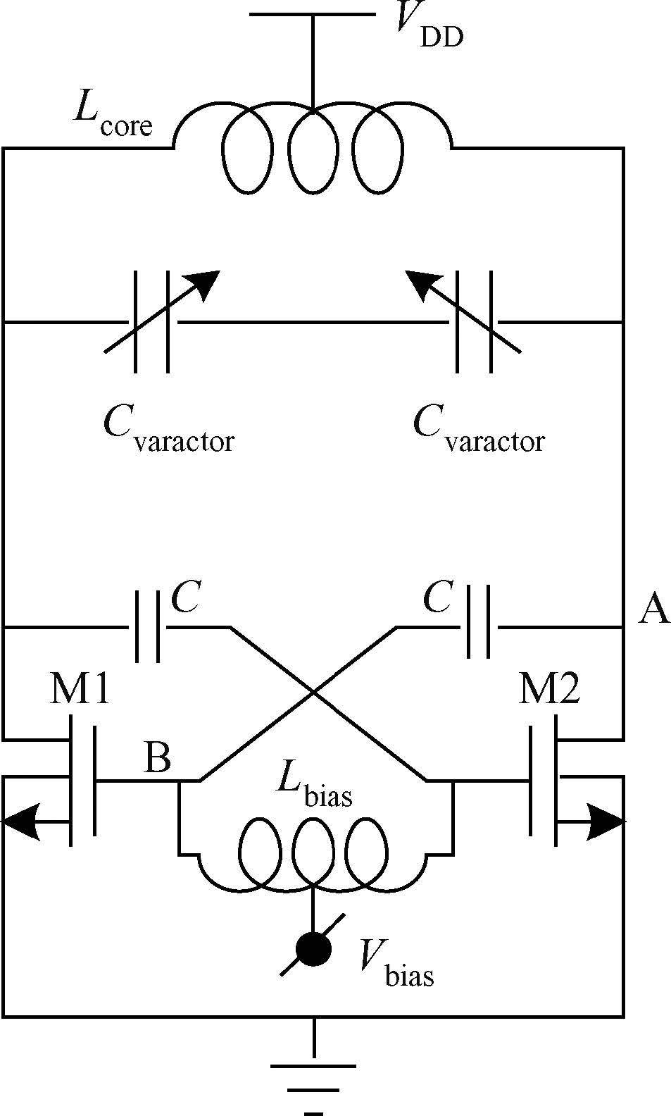
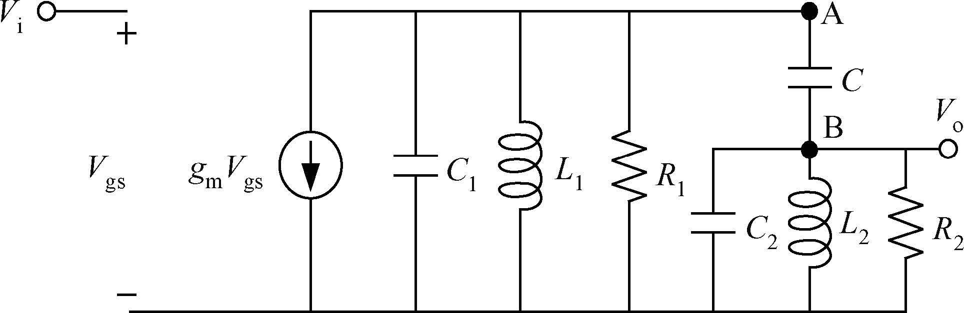
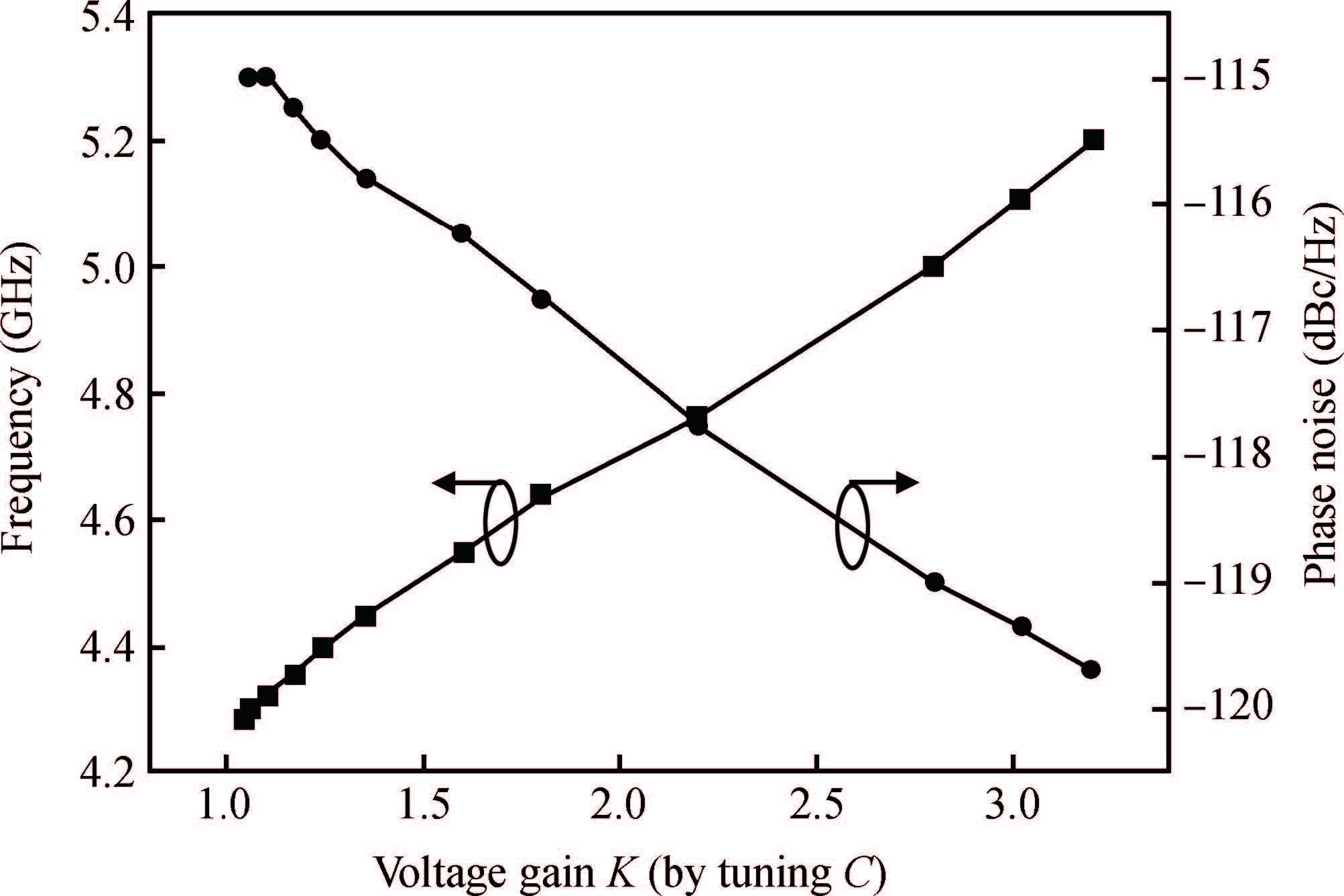
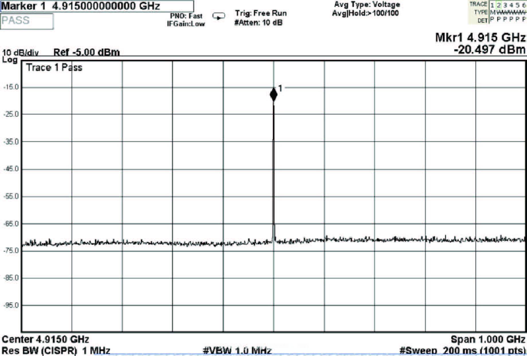
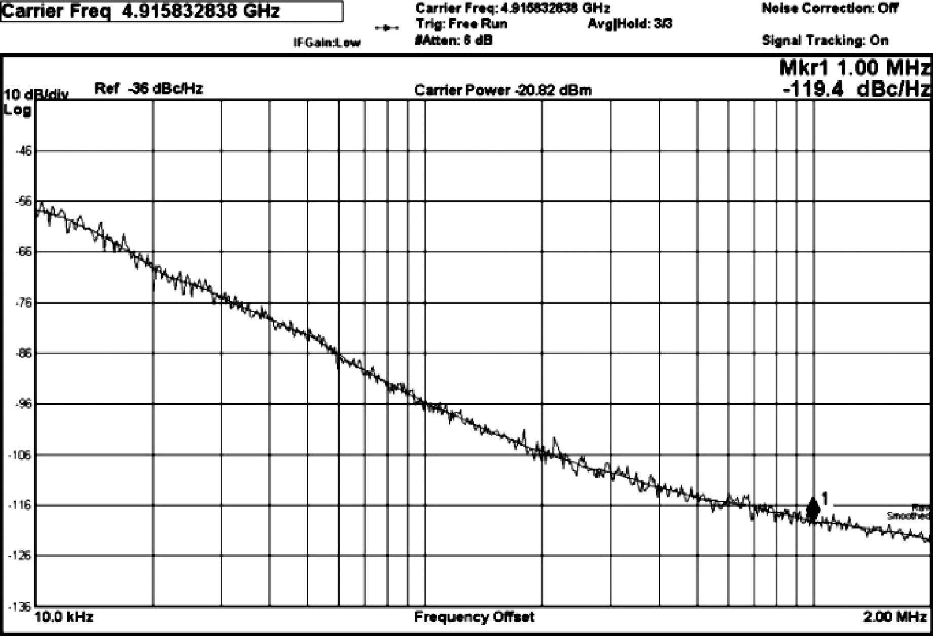
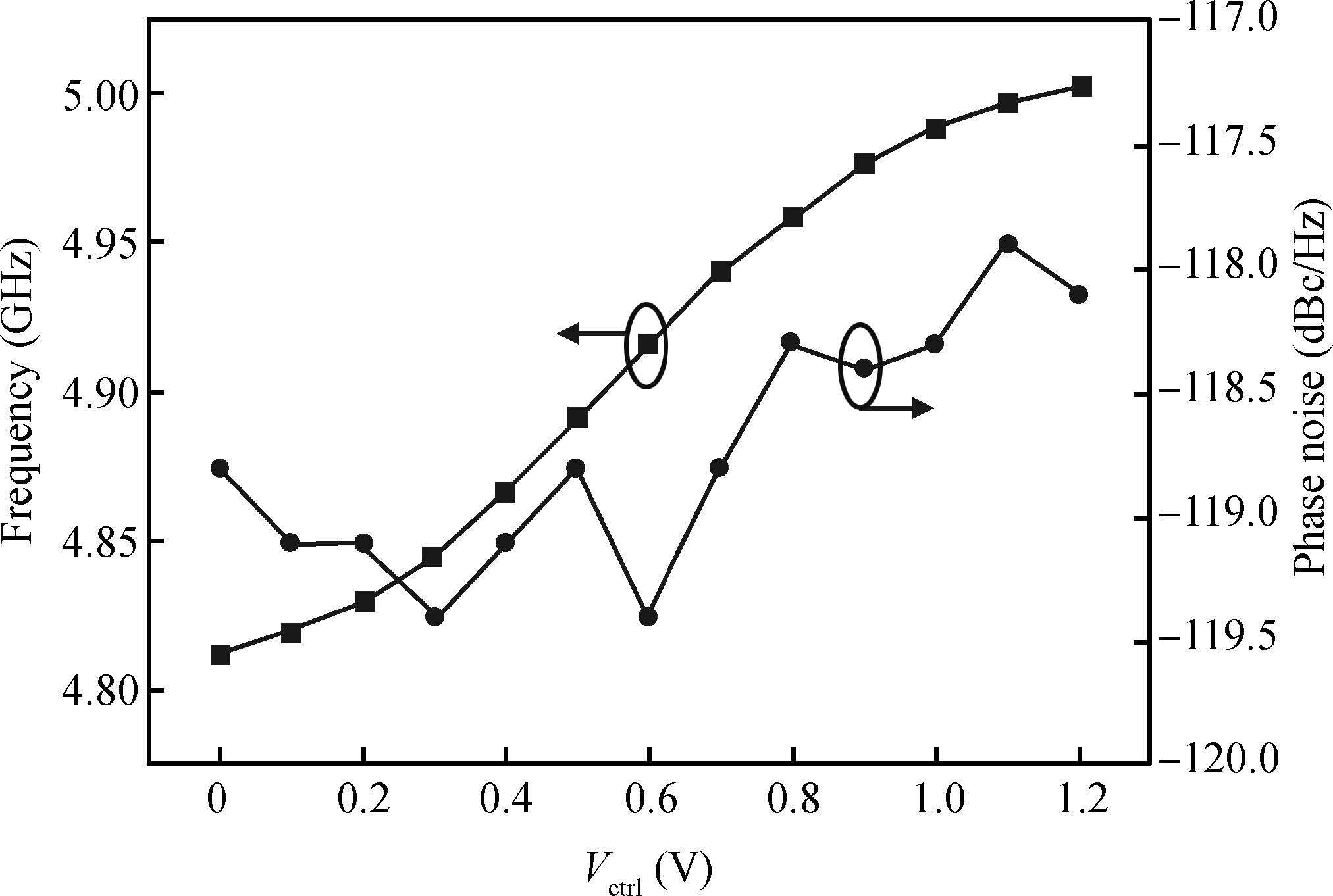
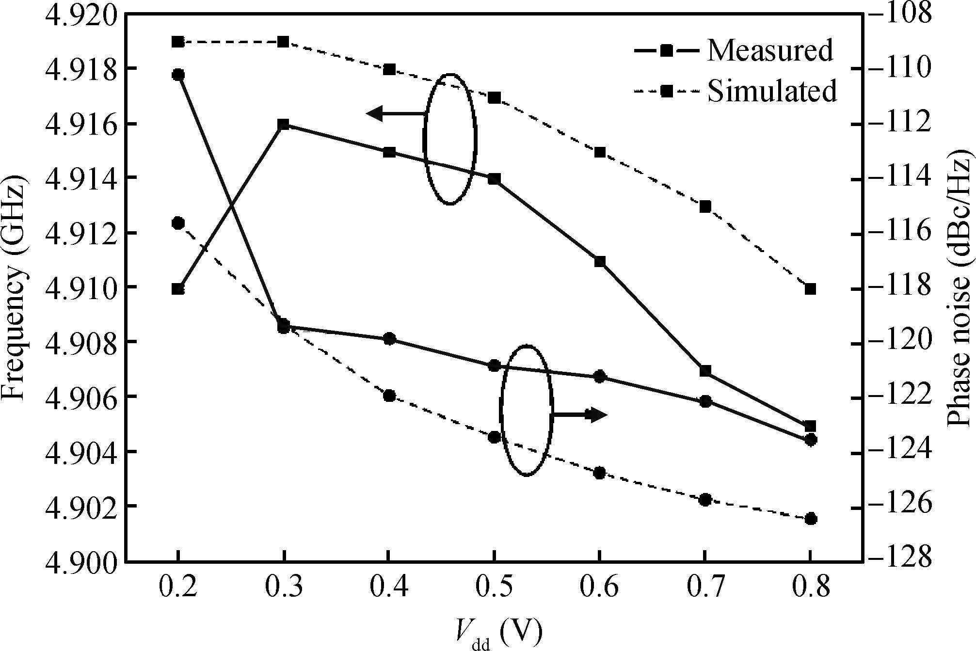
A novel voltage-controlled oscillator (VCO) topology with low voltage and low power is presented. It employed the inductive-biasing to build a feedback path between the tank and the MOS gate to enhance the voltage gain from output nodes of the tank to the gate node of the cross-coupled transistor. Theoretical analysis using time-varying phase noise theory derives closed-form symbolic formulas for the 1/f2 phase noise region, showing that this feedback path could improve the phase noise performance. The proposed VCO is fabricated in TSMC 0.13 μm CMOS technology. Working under a 0.3 V supply voltage with 1.2 mW power consumption, the measured phase noise of the VCO is -119.4 dBc/Hz at 1 MHz offset frequency from the carrier of 4.92 GHz, resulting in an FoM of 192.5 dBc/Hz.


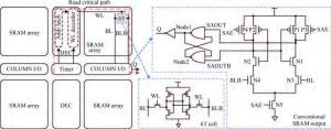
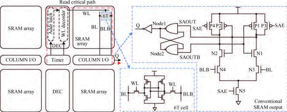
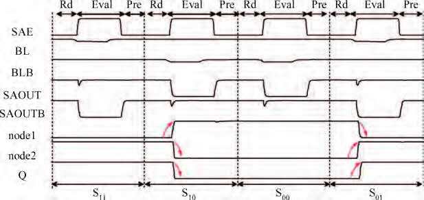
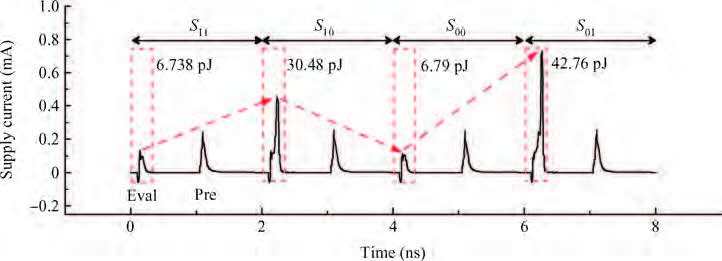
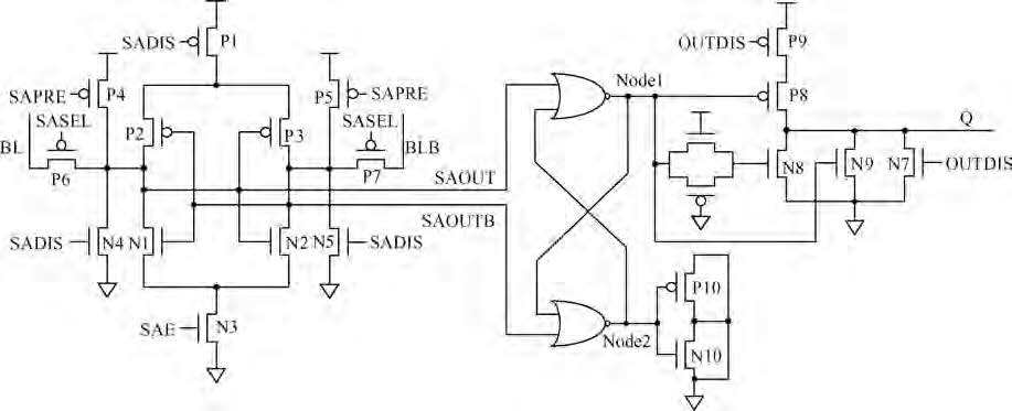
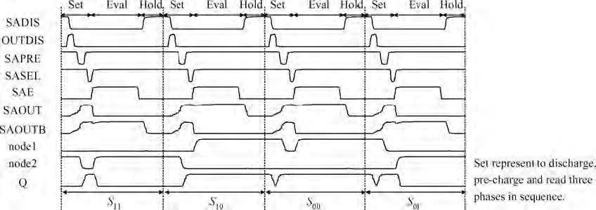
A power balance static random-access memory (SRAM) for resistance to differential power analysis (DPA) is proposed. In the proposed design, the switch power consumption and short-circuit power consumption are balanced by discharging and pre-charging the key nodes of the output circuit and adding an additional short-circuit current path. Thus, the power consumption is constant in every read cycle. As a result, the DPA-resistant ability of the SRAM is improved. In 65 nm CMOS technology, the power balance SRAM is fully custom designed with a layout area of 5863.6 μm2.The post-simulation results show that the normalized energy deviation (NED) and normalized standard deviation (NSD) are 0.099% and 0.04%, respectively. Compared to existing power balance circuits, the power balance ability of the proposed SRAM has improved 53%.


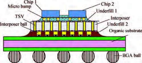
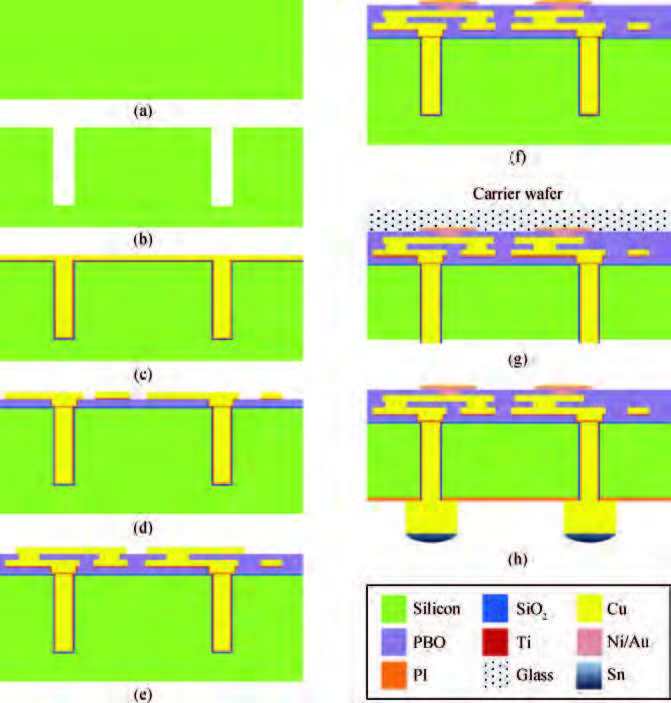
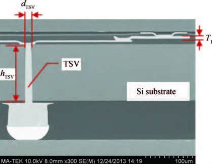
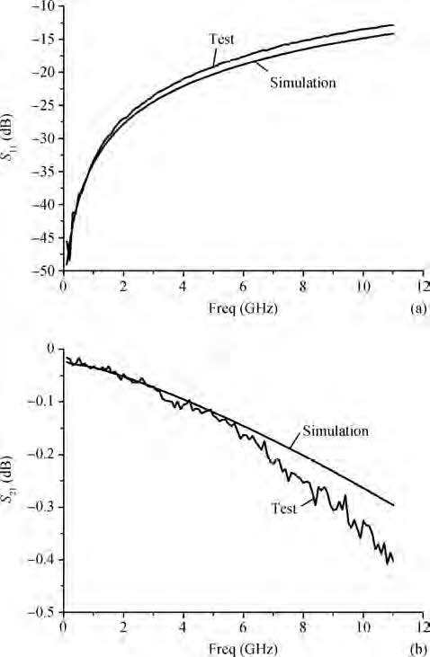
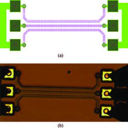
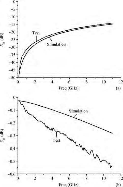
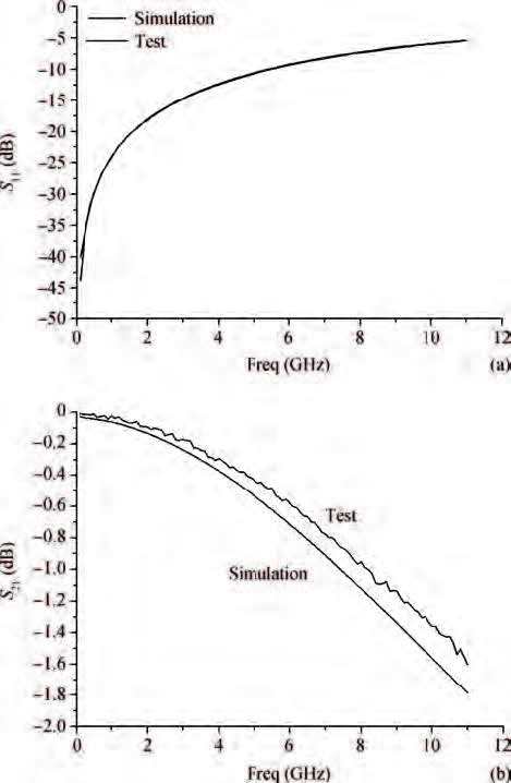
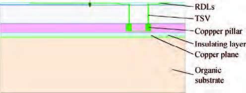
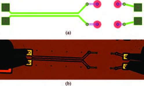
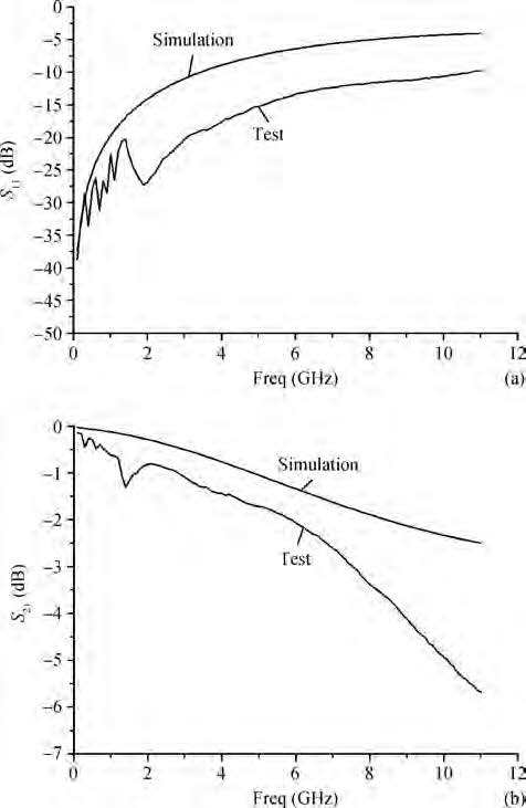
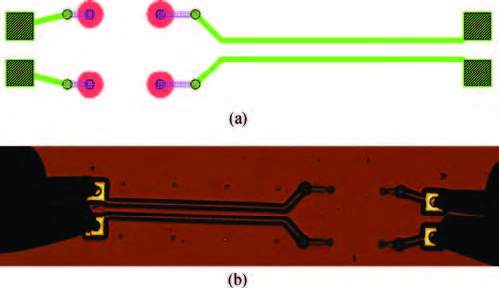
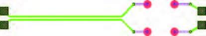
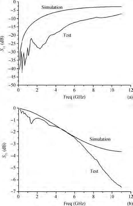
An interposer test vehicle with TSVs (through-silicon vias) and two redistribute layers (RDLs) on the top side for 2.5D integration was fabricated and high-frequency interconnections were designed in the form of coplanar waveguide (CPW) and micro strip line (MSL) structures. The signal transmission structures were modeled and simulated in a 3D EM tool to estimate the S-parameters. The measurements were carried out using the vector network analyzer (VNA). The simulated results of the transmission lines on the surface of the interposer without TSVs showed good agreement with the simulated results, while the transmission structures with TSVs showed significant offset between simulation and test results. The parameters of the transmission structures were changed, and the results were also presented and discussed in this paper.


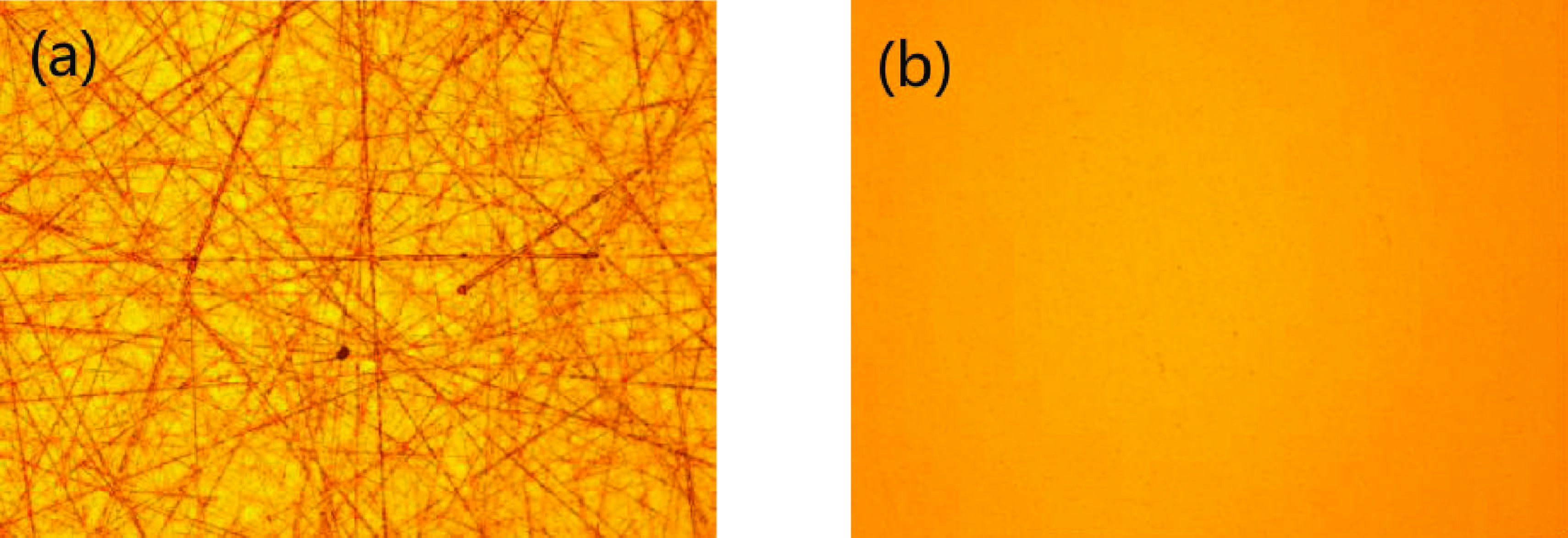
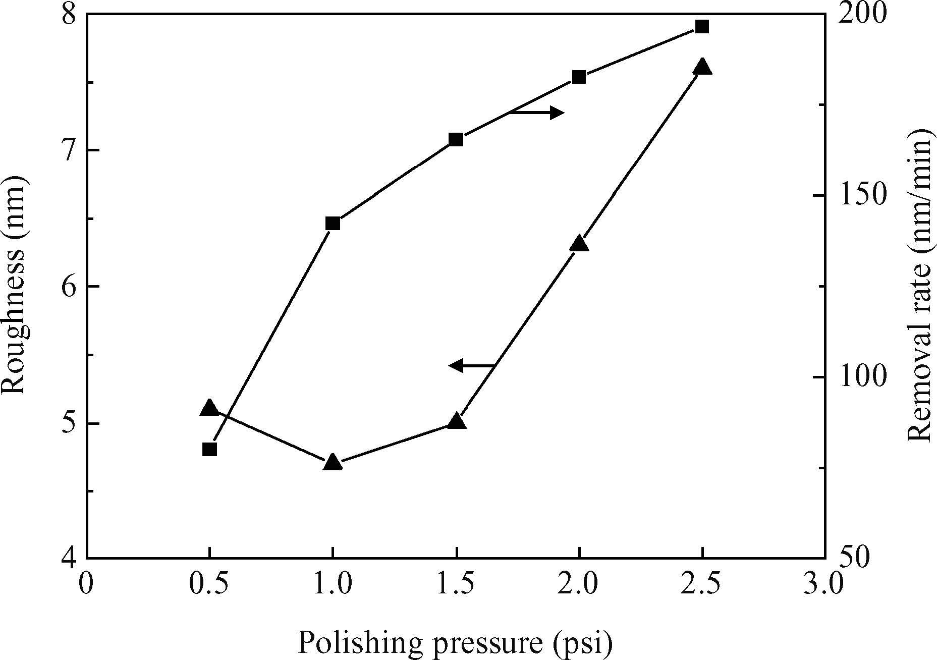
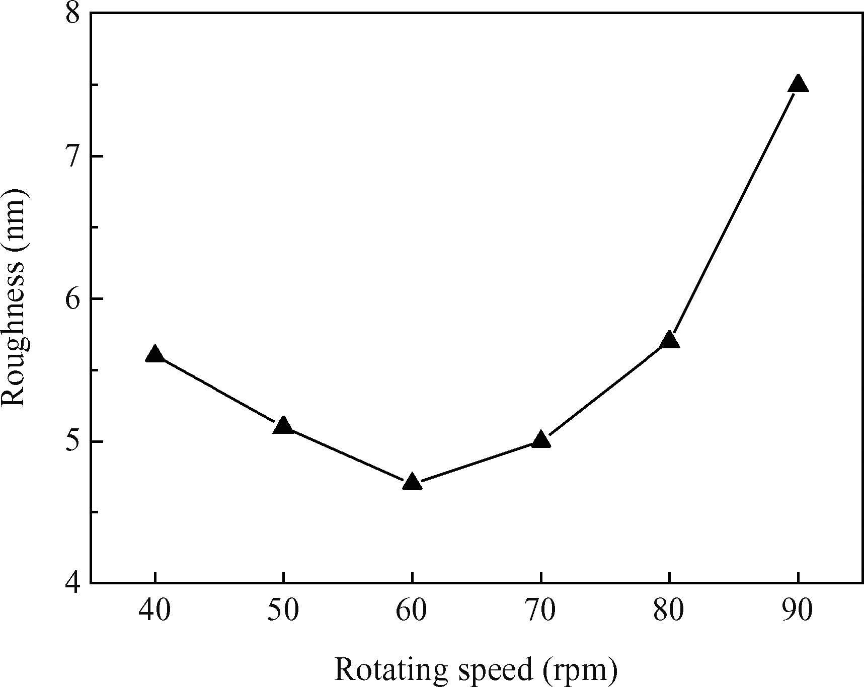
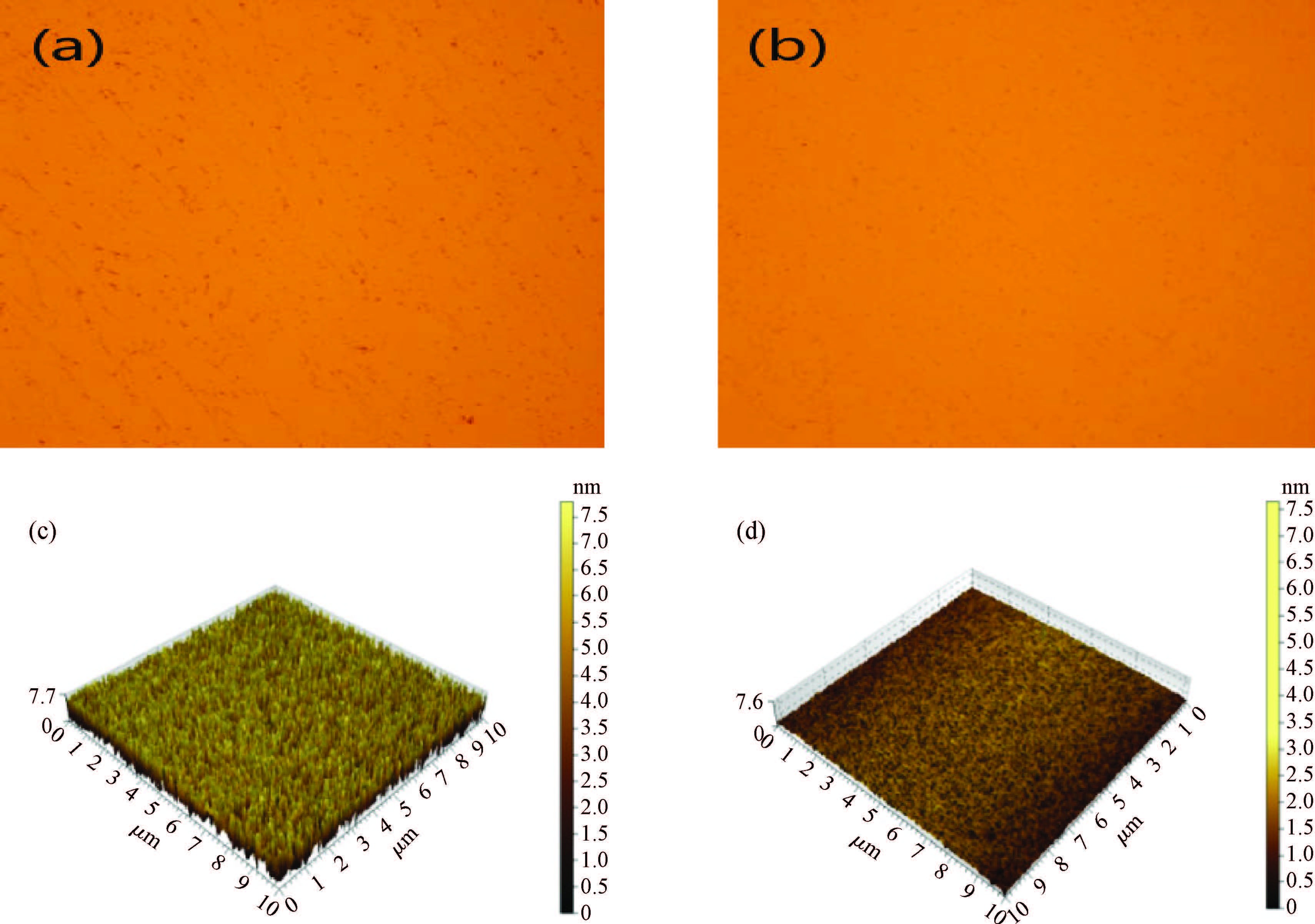
The replacement metal gate (RMG) defectivity performance control is very challenging in high-k metal gate (HKMG) chemical mechanical polishing (CMP). In this study, three major defect types, including fall-on particles, micro-scratch and corrosion have been investigated. The research studied the effects of polishing pad, pressure, rotating speed, flow rate and post-CMP cleaning on the three kinds of defect, which finally eliminated the defects and achieved good surface morphology. This study will provide an important reference value for the future research of aluminum metal gate CMP.