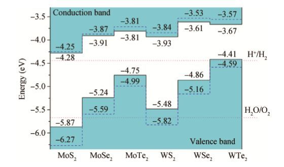
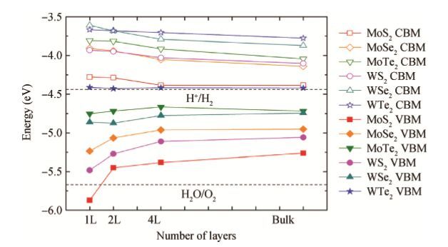
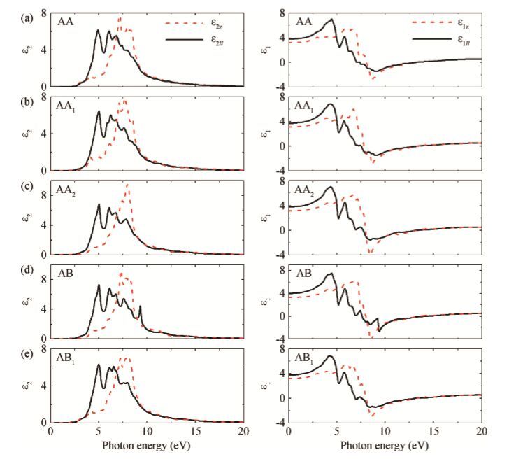
Since two-dimensional (2D) graphene was fabricated successfully, many kinds of graphene-like 2D materials have attracted extensive attention. Among them, the studies of 2D metal chalcogenides have become the focus of intense research due to their unique physical properties and promising applications. Here, we review significant recent advances in optoelectronic properties and applications of 2D metal chalcogenides. This review highlights the recent progress of synthesis, characterization and isolation of single and few layer metal chalcogenides nanosheets. Moreover, we also focus on the recent important progress of electronic, optical properties and optoelectronic devices of 2D metal chalcogenides. Additionally, the theoretical model and understanding on the band structures, optical properties and related physical mechanism are also reviewed. Finally, we give some personal perspectives on potential research problems in the optoelectronic characteristics of 2D metal chalcogenides and related device applications.


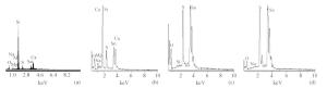
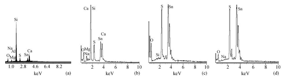
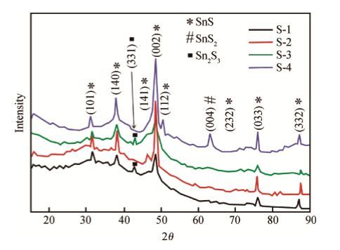
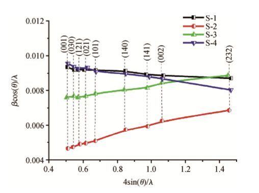
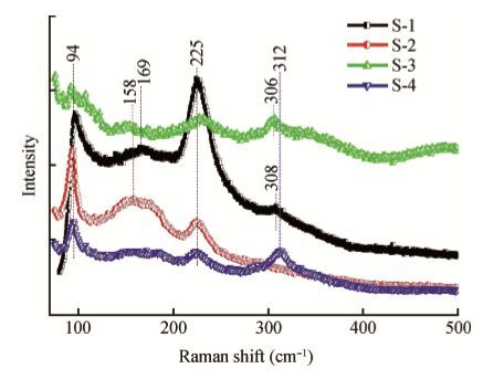
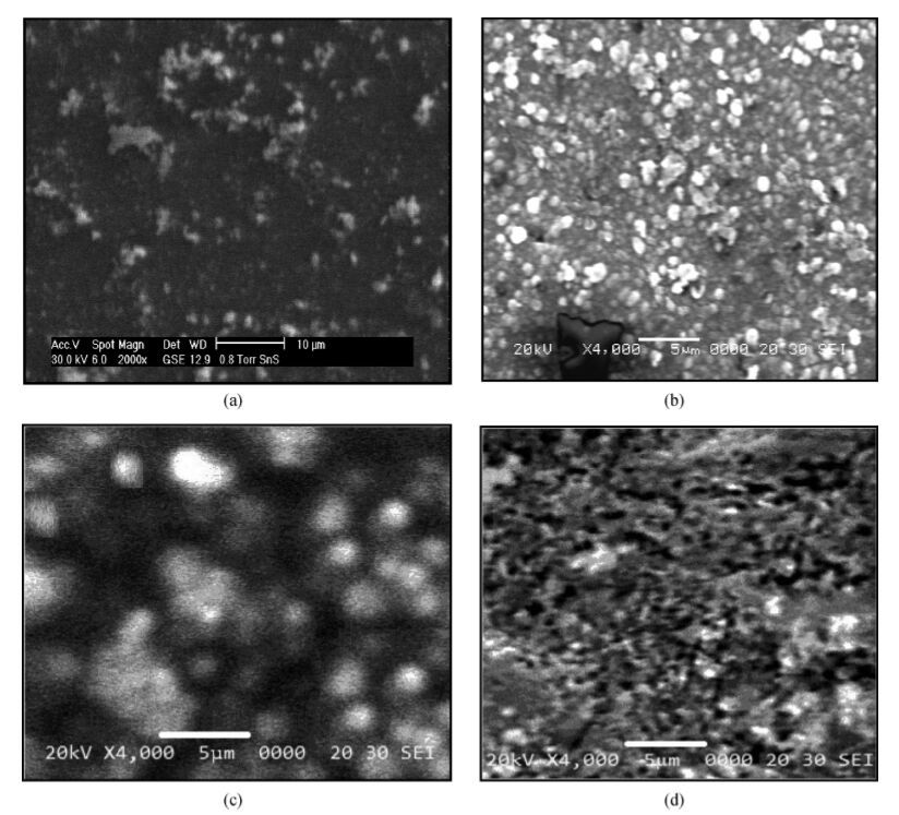
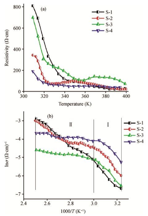
The SnS thin films were synthesized by chemical bath deposition (CBD), dip coating and successive ionic layer adsorption and reaction (SILAR) techniques. In them, the CBD thin films were deposited at two temperatures: ambient and 70 ℃. The energy dispersive analysis of X-rays (EDAX), X-ray diffraction (XRD), Raman spectroscopy, scanning electron microscopy (SEM) and optical spectroscopy techniques were used to characterize the thin films. The electrical transport properties studies on the as-deposited thin films were done by measuring the I-V characteristics, DC electrical resistivity variation with temperature and the room temperature Hall effect. The obtained results are deliberated in this paper.
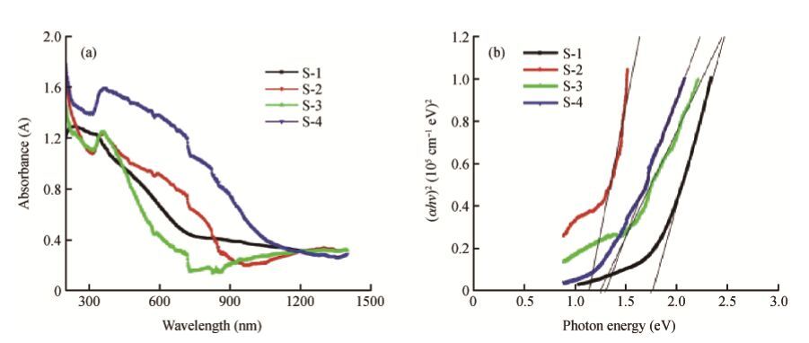
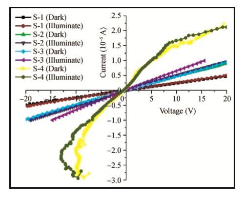
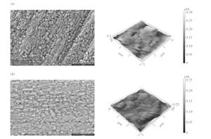
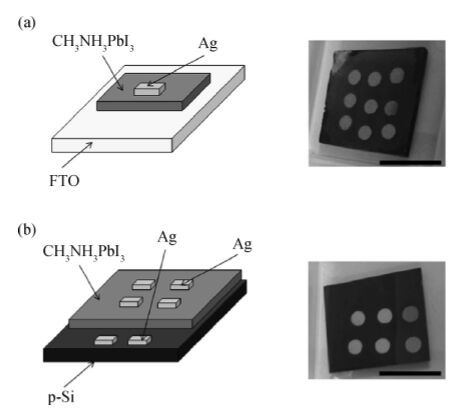
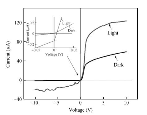
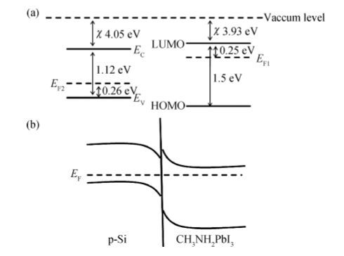
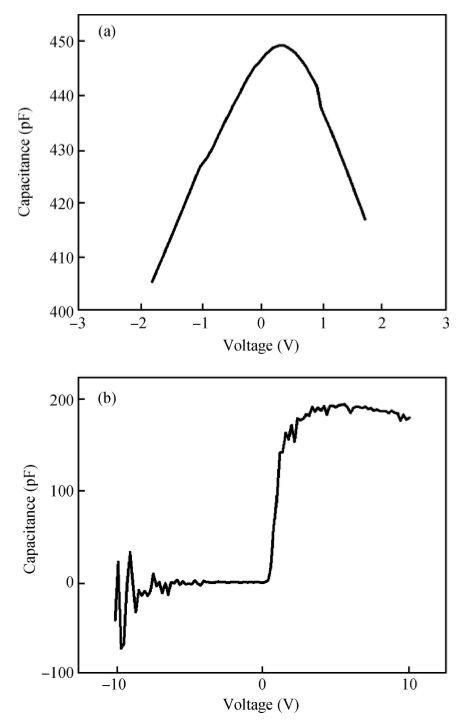
Organic-inorganic hybrid perovskite CH3NH3PbI3 film is prepared on p-type silicon substrate using the one-step solution method to form a CH3NH3PbI3/p-Si heterojunction. The film morphology and structure are characterized by atomic force microscopy (AFM) and scanning electron microscopy (SEM). The photoelectric properties of the CH3NH3PbI3/p-Si heterojunction are studied by testing the current-voltage (I-V) with and without illumination and capacitance-voltage (C-V) characteristics. It turns out from the I-V curve without illumination that the CH3NH3PbI3/p-Si heterojunction has a rectifier feature with the rectification ratio over 70 at the bias of ± 5 V. Also, there appears a photoelectric conversion phenomenon on this heterojunction with a short circuit current (Im sc) of 0.16 μA and an open circuit voltage (Voc) of about 10 mV. The high frequency C-V characteristic of the Ag/CH3NH3PbI3/p-Si heterojunction turns out to be similar to that of the metal-insulator-semiconductor (MIS) structure, and a parallel translation of the C-V curve along the forward voltage axis is found. This parallel translation means the existence of defects at the CH3NH3PbI3/p-Si interface and positive fixed charges in the CH3NH3PbI3 layer. The defects at the interface of the CH3NH3PbI3/p-Si heterojunction result in the dramatic decline of the Voc. Besides, the C-V test of CH3NH3PbI3 film shows a non-linear dielectric property and the dielectric value is about 4.64 as calculated.


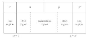
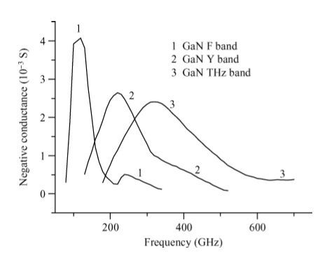
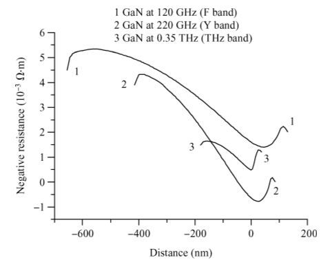
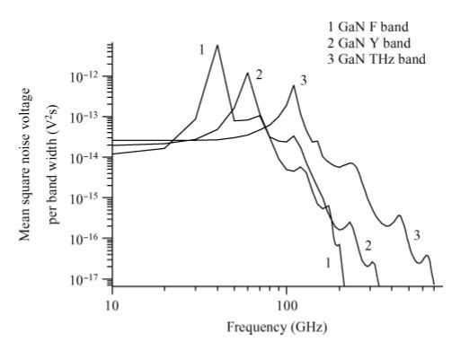
The potential of GaN as a wide band gap semiconductor is explored for application as double drift region mixed tunneling avalanche transit time (MITATT) diodes for operation at 120 GHz, 220 GHz and 0.35 THz using some computer simulation methods developed by our group. The salient features of our results have uncovered some peculiarities of the GaN based MITATT devices. An efficiency of more than 20% right up to a frequency of 0.35 THz (from the GaN MITATT diode) seems highly encouraging but a power output of only 0.76 W is indicative of its dismal fate. The existence of a noise measure minimum at the operating frequency of 0.35 THz is again exhilarating but the value of the minimum is miserably high i.e. more than 33 dB. Thus, although GaN is a wide band gap semiconductor, the disparate carrier velocities prevent its full potential from being exploited for application as MTATT diodes.

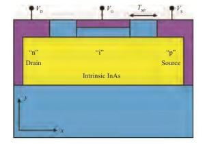
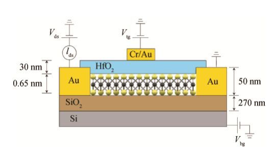
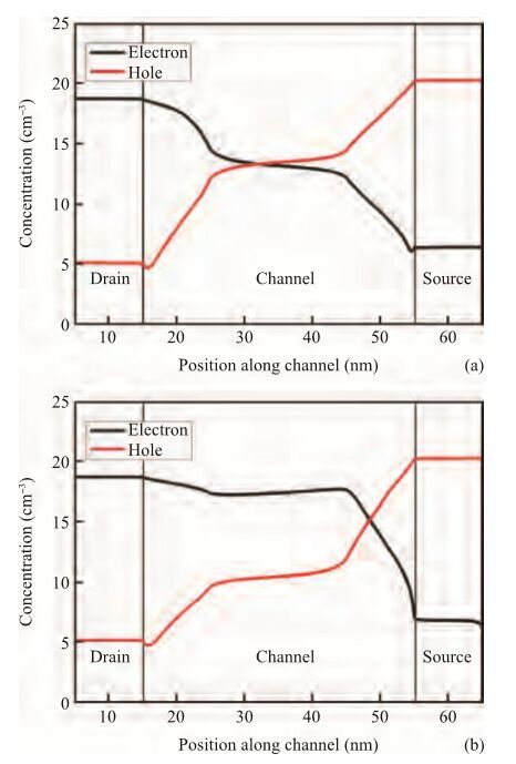
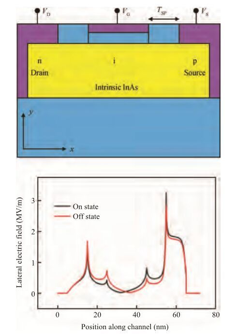
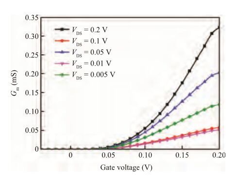
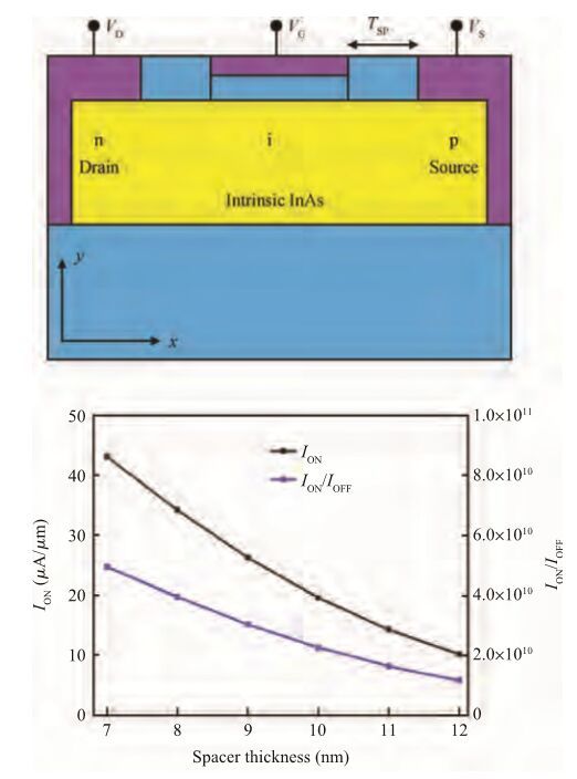
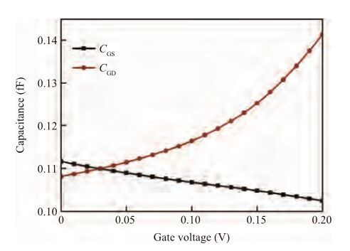
We propose a nanoscale single gate ultra thin body intrinsic channel tunnel field effect transistor using the charge plasma concept for ultra low power applications. The characteristics of TFETs (having low leakage) are improved by junctionless TFETs through blending advantages of Junctionless FETs (with high on current). We further improved the characteristics, simultaneously simplifying the structure at a very low power rating using an InAs channel. We found that the proposed device structure has reduced short channel effects and parasitics and provides high speed operation even at a very low supply voltage with low leakage. Simulations resulted in IOFF of ~ 9 × 10-16A/μm, ION of ~20 μA/μm, ION/IOFF of ~2 × 10¹⁰, threshold voltage of 0.057 V, subthreshold slope of 7 mV/dec and DIBL of 86 mV/V for PolyGate/HfO2/InAs TFET at a temperature of 300 K, gate length of 20 nm, oxide thickness of 2 nm, film thickness of 10 nm, low-k spacer thickness of 10 nm and VDD of 0.2 V.


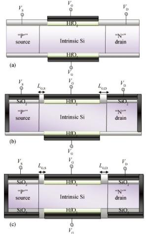
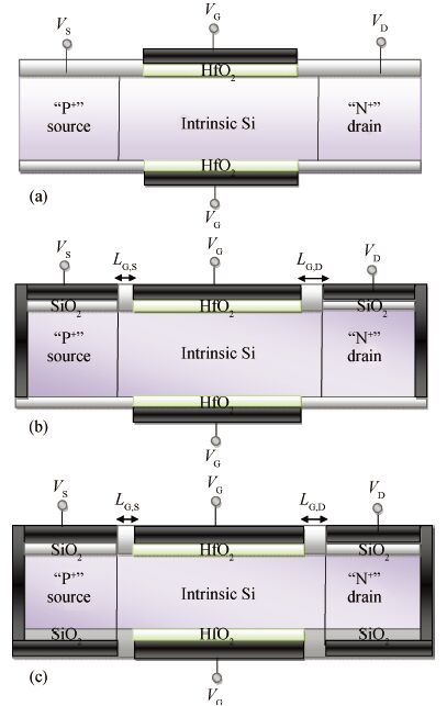
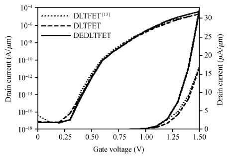
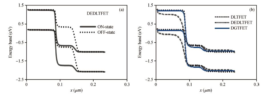
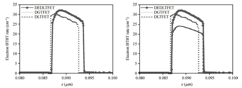
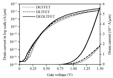
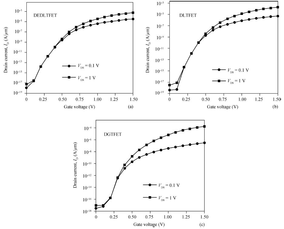
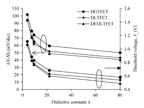
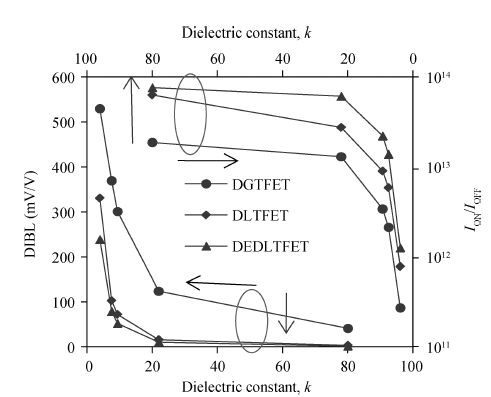
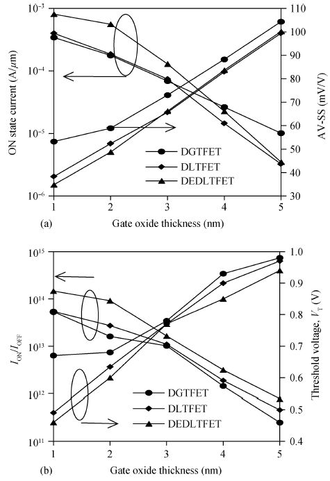
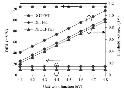
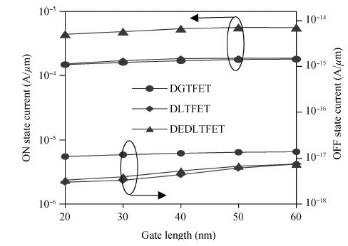
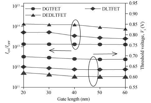
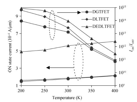
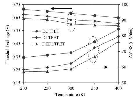
This paper proposes the charge plasma based dual electrode doping-less tunnel FET (DEDLTFET). The paper compares the device performance of the conventional doping-less TFET (DLTFET) and doped TFET (DGTFET). DEDLTEFT gives the superior results with high ON state current (ION ~ 0.56 mA/μm), ION/IOFF ratio ~ 9.12 × 10¹³ and an average subthreshold swing (AV-SS ~ 48 mV/dec). The variation of different device parameters such as channel length, gate oxide material, gate oxide thickness, silicon thickness, gate work function and temperature variation are done and compared with DLTFET and DGTFET. Through the extensive analysis it is found that DEDLTFET shows the better performance than the other two devices, which gives the indication for an excellent future in low power applications.


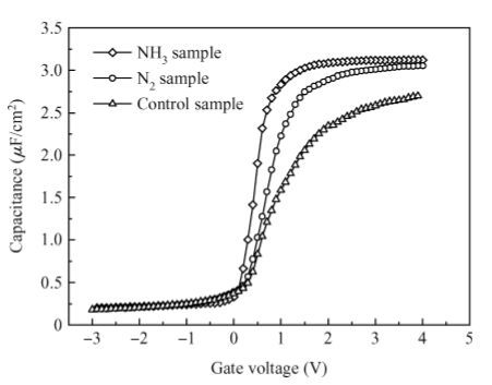
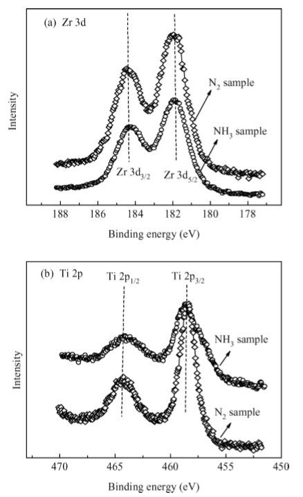
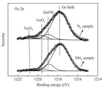
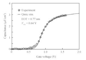
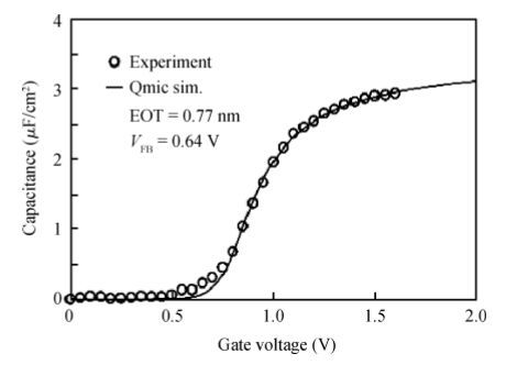
The interfacial and electrical characteristics of Ge metal-oxide-semiconductor (MOS) devices with a dual passivation layer of ZrON/GeON formed by NH3- or N2-plasma treatment are investigated. The experimental results show that the NH3-plasma treated sample exhibits significantly improved interfacial and electrical properties as compared to the samples with N2-plasma treatment and no treatment: a lower interface-state density at the midgap (1.64 × 1011 cm-2·eV-1) and gate leakage current (9.32 × 10⁻⁵ A/cm2 at Vfb+ 1 V), a small capacitance equivalent thickness (1.11 nm) and a high k value (32). X-ray photoelectron spectroscopy is used to analyze the involved mechanisms. It is indicated that more GeON and less GeOx (x <2) are formed on the Ge surface during NH3-plasma treatment than the N2-plasma treatment, resulting in a high-quality high-k/Ge interface, because H atoms and NH radicals in NH3-plasma can enhance volatilization of the unstable low-k GeOx, creating high-quality GeON passivation layer. Moreover, more nitrogen incorporation in ZrON/GeON induced by NH3-plasma treatment can build a stronger N barrier and thus more effectively inhibit in-diffusion of O and Ti from high-k gate dielectric and out-diffusion of Ge.


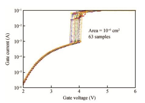
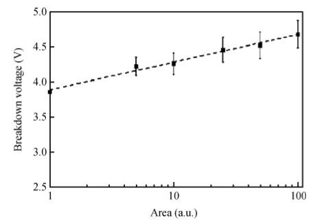
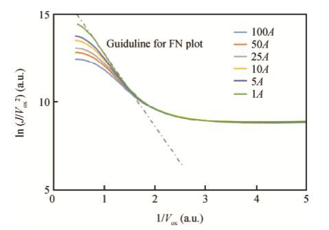
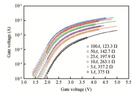
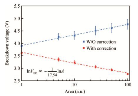
The time zero dielectric breakdown characteristics of MOSCAP with ultra-thin EOT high-k metal gate stacks are studied. The TZDB results show an abnormal area dependence due to the series resistance effect. The series resistance components extracted from the Fowler-Nordheim tunneling relation are attributed to the spreading resistance due to the asymmetry electrodes. Based on a series model to eliminate the series resistance effect, an area acceleration dependence is obtained by correcting the TZDB results. The area dependence follows Poisson area scaling rules, which indicates that the mechanism of TZDB is the same as TDDB and could be considered as a trap generation process.

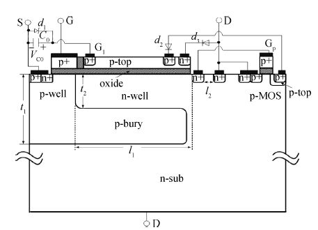
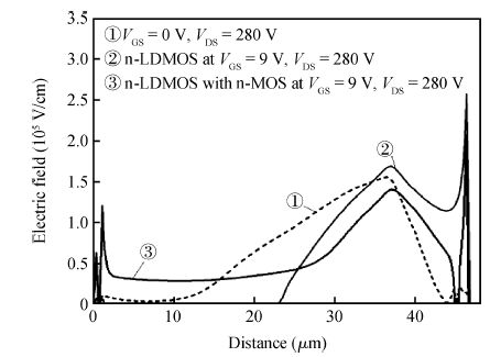
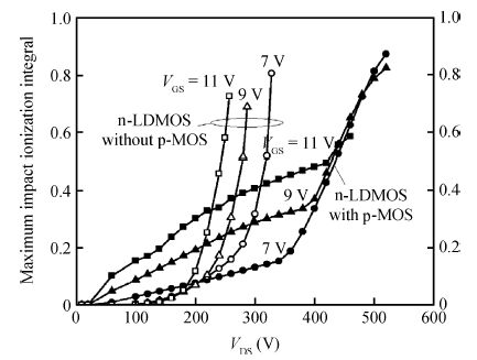
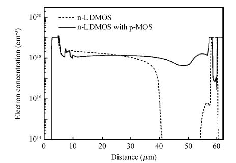
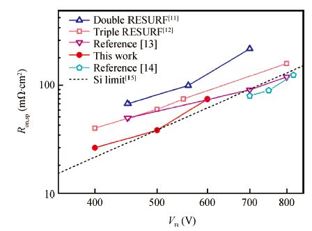
An LDMOS with nearly rectangular-shape safe operation area (SOA) and low specific on-resistance is proposed. By utilizing a split gate, an electron accumulation layer is formed near the surface of the n-drift region to improve current conduction capability during on-state operation. As a result, the specific on-resistance can be lowered down to 74.7 mΩ·cm2 for a 600 V device from simulation. Furthermore, under high-voltage and high-current conditions, electrons and holes flow as majority carriers in the n-drift region and p-type split gate, respectively. Due to charge compensation occurring between holes and electrons, the local electric field is reduced and impact ionization is weakened in the proposed device. Therefore, a higher on-state breakdown voltage at large VGS is obtained and snap-back is suppressed as well.


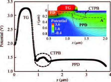
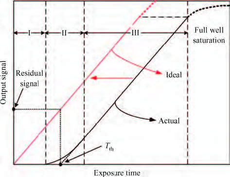
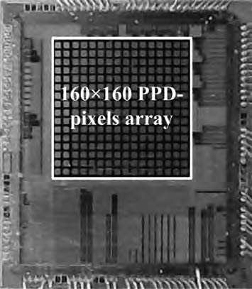
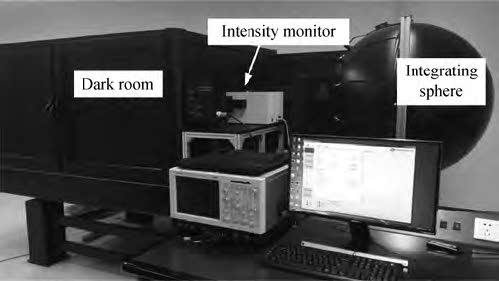
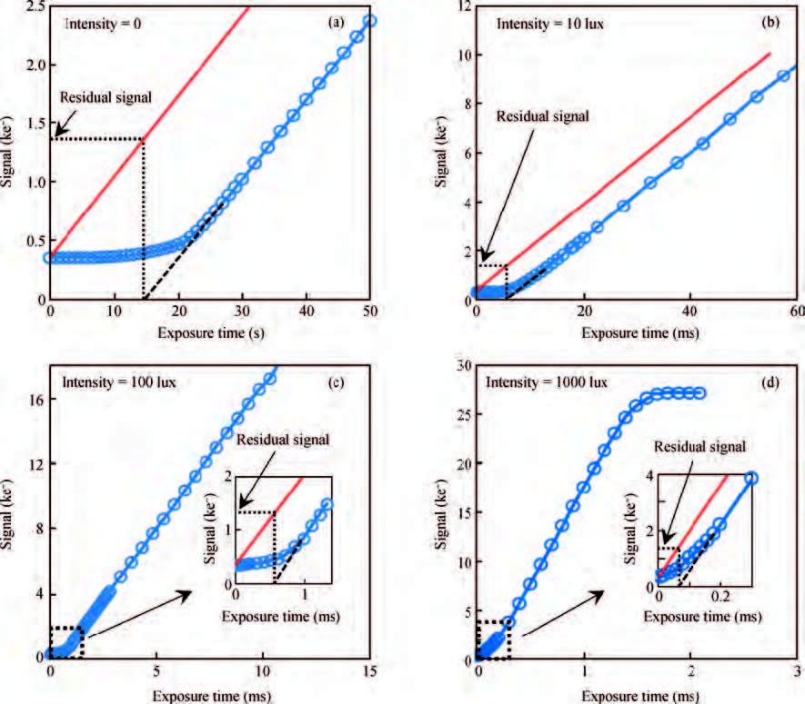
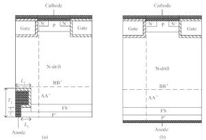
The charge transfer potential barrier (CTPB) formed beneath the transfer gate causes a noticeable image lag issue in pinned photodiode (PPD) CMOS image sensors (CIS), and is difficult to measure straightforwardly since it is embedded inside the device. From an understanding of the CTPB formation mechanism, we report on an alternative method to feasibly measure the CTPB height by performing a linear extrapolation coupled with a horizontal left-shift on the sensor photoresponse curve under the steady-state illumination. The theoretical study was performed in detail on the principle of the proposed method. Application of the measurements on a prototype PPD-CIS chip with an array of 160 × 160 pixels is demonstrated. Such a method intends to shine new light on the guidance for the lag-free and high-speed sensors optimization based on PPD devices.


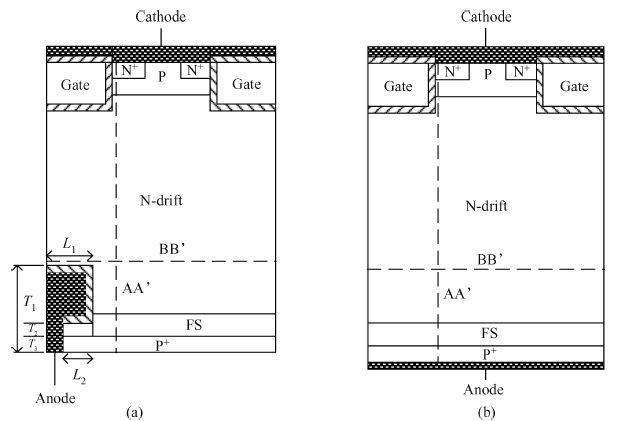
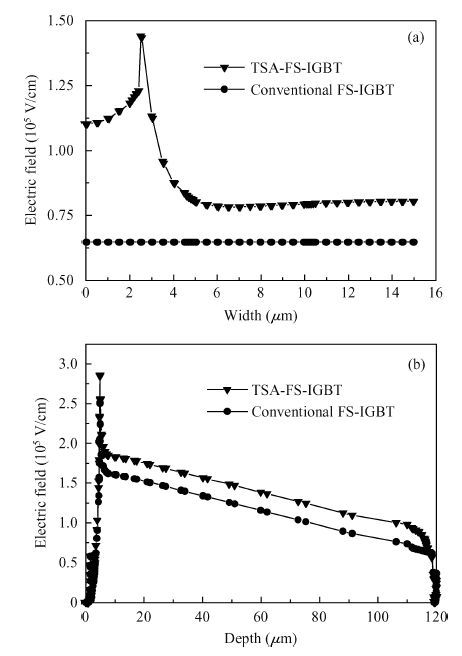
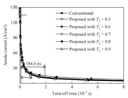
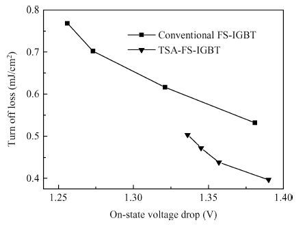
A novel trench field stop (FS) insulated gate bipolar transistor (IGBT) with a trench shorted anode (TSA) is proposed. By introducing a trench shorted anode, the TSA-FS-IGBT can obviously improve the breakdown voltage. As the simulation results show, the breakdown voltage is improved by a factor of 19.5% with a lower leakage current compared with the conventional FS-IGBT. The turn off time of the proposed structure is 50% lower than the conventional one with less than 9% voltage drop increased at a current density of 150 A/cm2. Additionally, there is no snapback observed. As a result, the TSA-FS-IGBT has a better trade-off relationship between the turn off loss and forward drop.


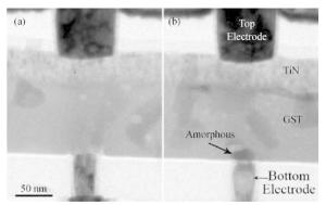
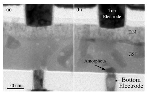
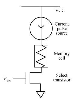
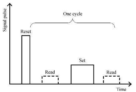
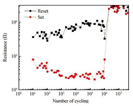
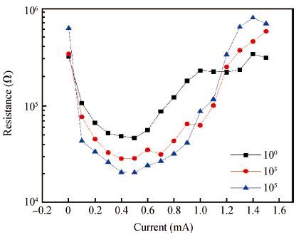
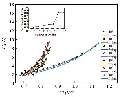
The endurance characteristics of phase change memory are studied. With operational cycles, the resistances of reset and set states gradually change to the opposite direction. What is more, the operational conditions that are needed are also discussed. The failure and the changes are concerned with the compositional change of the phase change material. An abnormal phenomenon that the threshold voltage decreases slightly at first and then increases is observed, which is due to the coaction of interface contact and growing active volume size changing.


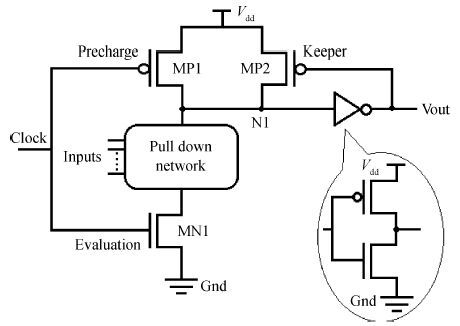
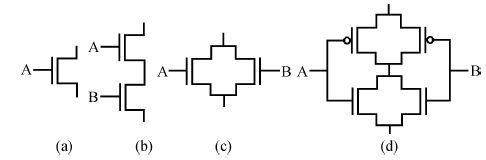
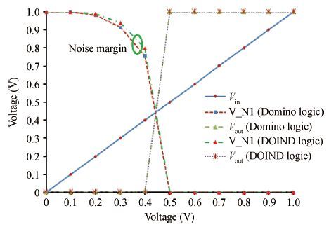
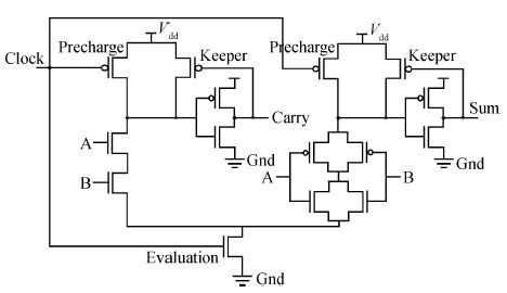
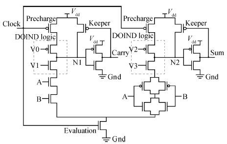
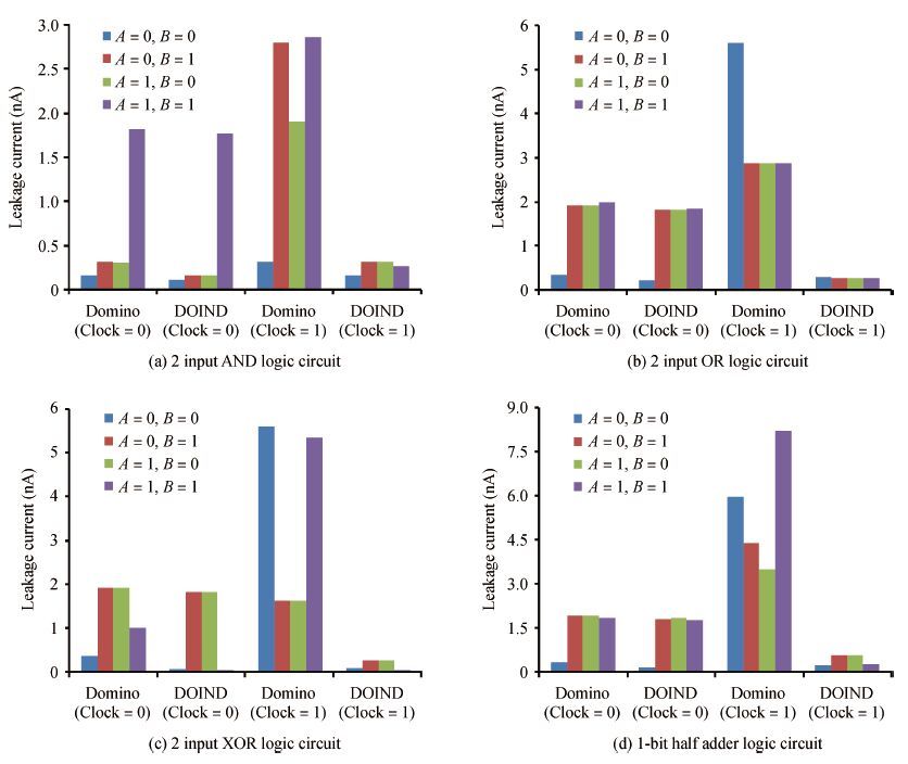
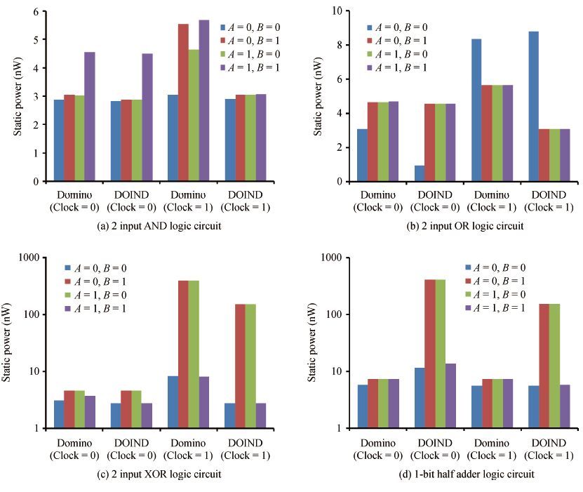
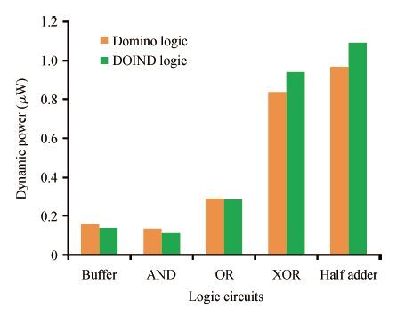
A novel DOIND logic approach is proposed for domino logic, which reduces the leakage current with a minimum delay penalty. Simulation is performed at 70 nm technology node with supply voltage 1V for domino logic and DOIND logic based AND, OR, XOR and Half Adder circuits using the tanner EDA tool. Simulation results show that the proposed DOIND approach decreases the average leakage current by 68.83%, 66.6%, 77.86% and 74.34% for 2 input AND, OR, XOR and Half Adder respectively. The proposed approach also has 47.76% improvement in PDAP for the buffer circuit as compared to domino logic.


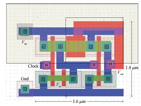

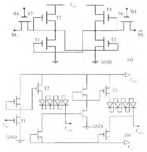
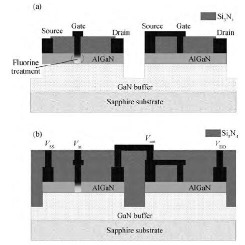
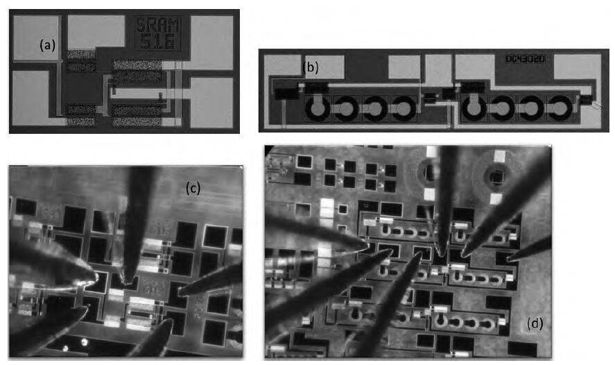
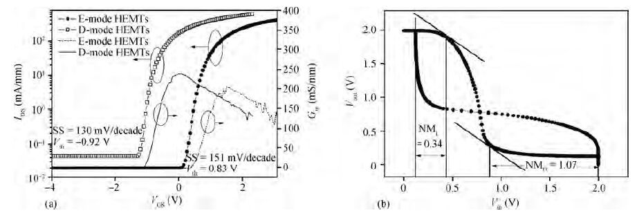
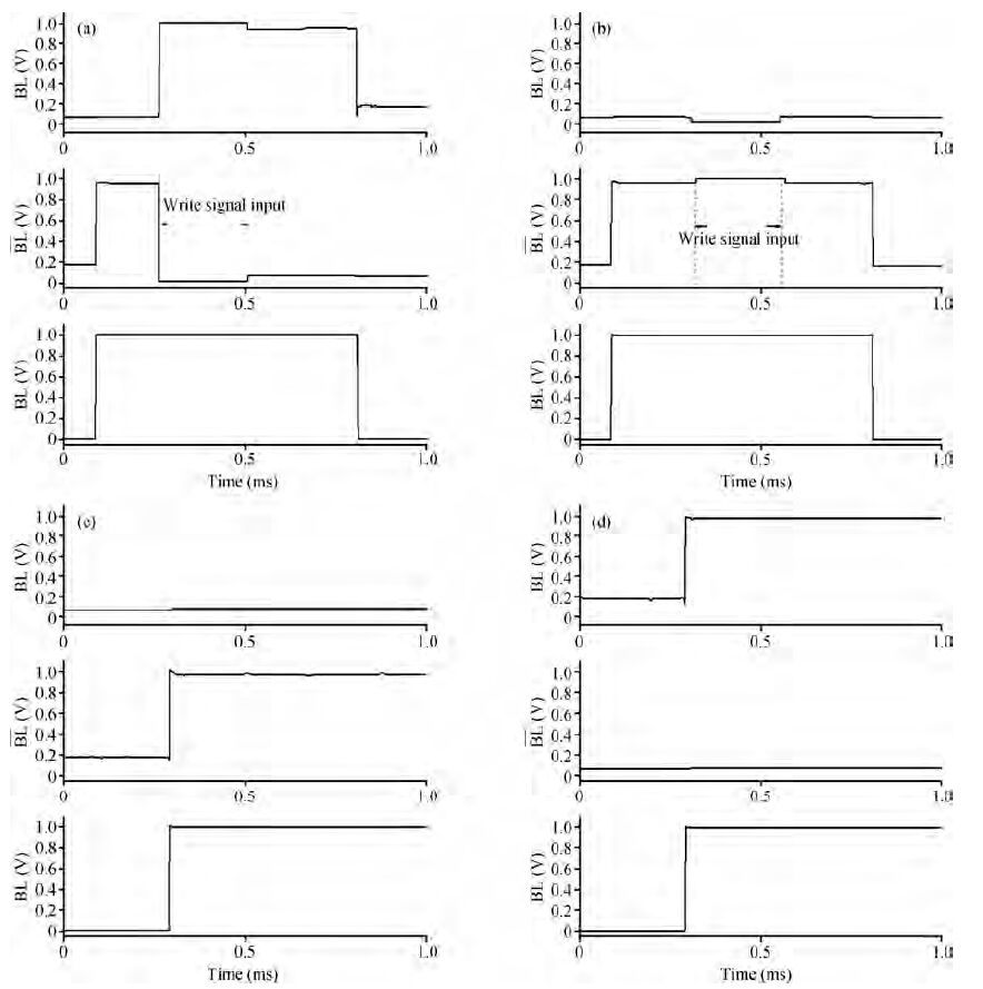
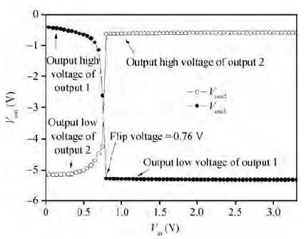
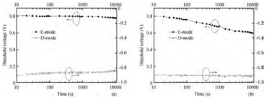
A GaN-based E/D mode direct-couple logic 6 transistors SRAM unit and a voltage level shifter were designed and fabricated. E-mode and D-mode AlGaN/GaN HEMTs were integrated in one wafer using fluorine plasma treatment and using a moderate AlGaN barrier layer heterojunction structure. The 6 transistors SRAM unit consists of two symmetrical E/D mode inverters and two E-mode switch HEMTs. The output low and high voltage of the SRAM unit are 0.95 and 0.07 V at a voltage supply of 1 V. The voltage level shifter lowers the supply voltage using four Ni-AlGaN Schottky diodes in a series at a positive supply voltage of 6 V and a negative supply voltage of -6 V. By controlling the states of inverter modules of the level shifter in turn, the level shifter offers two channel voltage outputs of -0.5 and -5 V. The flip voltage of the level shifter is 0.76 V. Both the SRAM unit and voltage shifter operate correctly, demonstrating the promising potential for GaN-based E/D mode digital and analog integrated circuits. Several considerations are proposed to avoid the influence of threshold voltage degradation of D-mode and E-mode HEMT on the operation of the circuit.

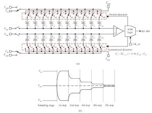
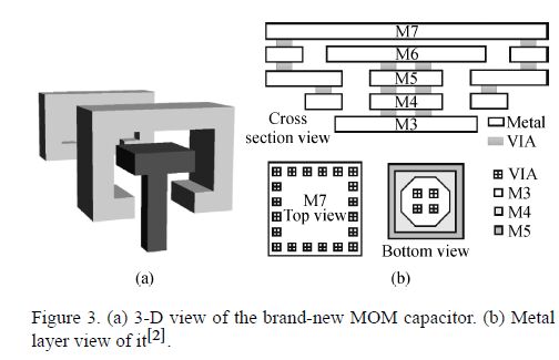
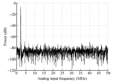
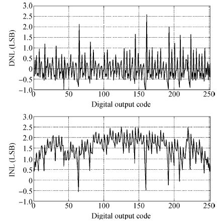
A low power 9 bit 100 MS/s successive approximation register analog-to-digital converter (SAR ADC) with custom capacitor array is presented. A brand-new 3-D MOM unit capacitor is used as the basic capacitor cell of this capacitor array. The unit capacitor has a capacitance of 1 fF. Besides, the advanced capacitor array structure and switch mode decrease the power consumption a lot. To verify the effectiveness of this low power design, the 9 bit 100 MS/s SAR ADC is implemented in TSMC IP9M 65 nm LP CMOS technology. The measurement results demonstrate that this design achieves an effective number of bits (ENOB) of 7.4 bit, a signal-to-noise plus distortion ratio (SNDR) of 46.40 dB and a spurious-free dynamic range (SFDR) of 62.31 dB at 100 MS/s with 1 MHz input. The SAR ADC core occupies an area of 0.030 mm2 and consumes 0.43 mW under a supply voltage of 1.2 V. The figure of merit (FOM) of the SAR ADC achieves 23.75 fJ/conv.


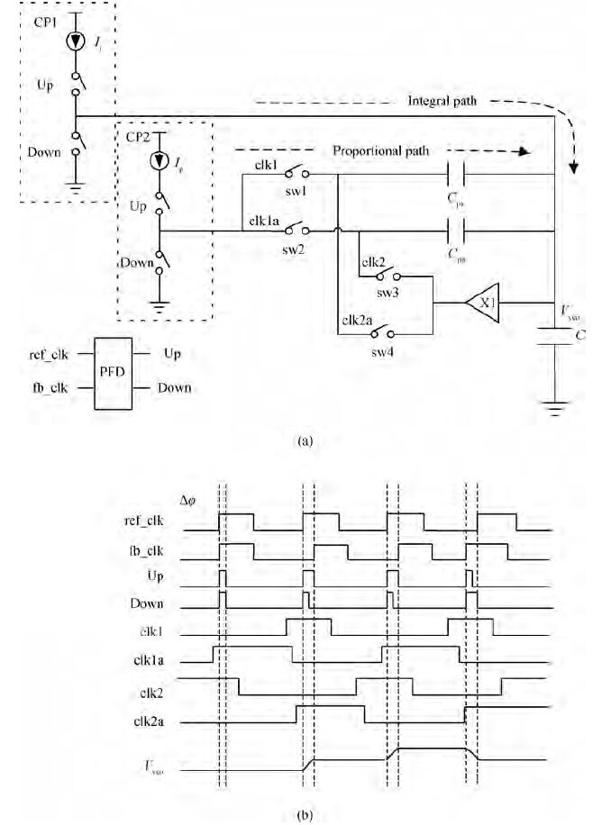
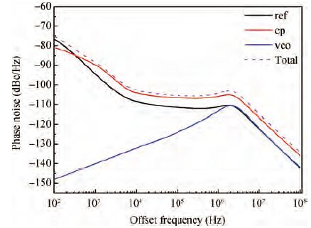
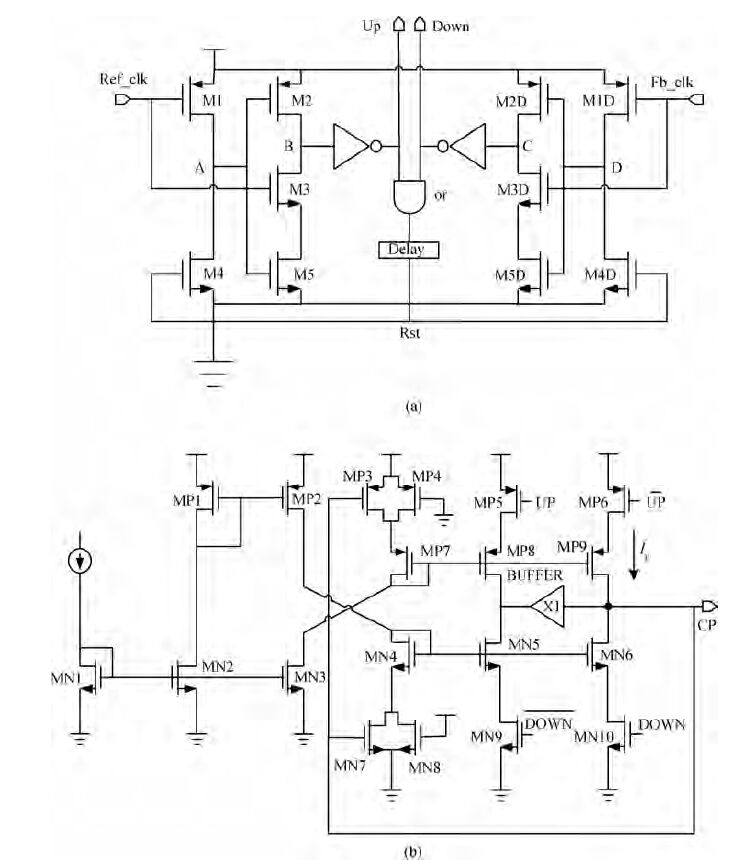
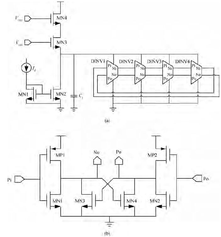
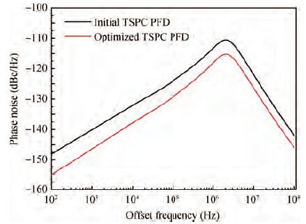
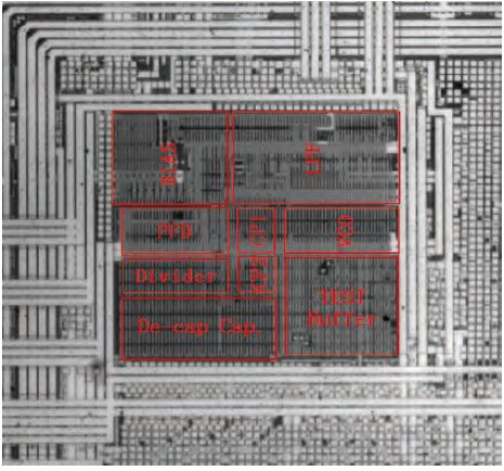
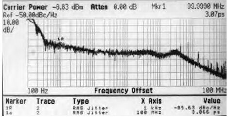
A 0.1-1.5 GHz, 3.07 pS root mean squares (RMS) jitter, area efficient phase locked loop (PLL) with multiphase clock outputs is presented in this paper. The size of capacitor in the low pass filter (LPF) is significantly decreased by implementing a dual path charge pump (CP) technique in this PLL. Subject to specified power consumption, a novel optimization method is introduced to optimize the transistor size in the voltage control oscillator (VCO), CP and phase/frequency detector (PFD) in order to minimize clock jitter. This method could improve 3-6 dBc/Hz phase noise. The proposed PLL has been fabricated in 55 nm CMOS process with an integrated 16 pF metal-oxide-metal (MOM) capacitor, occupies 0.05 mm2 silicon area, the measured total power consumption is 2.8 mW @ 1.5 GHz and the phase noise is -102 dBc/Hz @ 1 MHz offset frequency.

A new mixed curvature compensation technique for CMOS voltage reference is presented, which resorts to two sub-references with complementary temperature characteristics. The first sub-reference is the source-gate voltage |VGS|p of a PMOS transistor working in the saturated region. The second sub-reference is the weighted sum of gate-source voltages |VGS|n of NMOS transistors in the subthreshold region and the difference between two base-emitter voltages ΔVBE of bipolar junction transistors (BJTs). The voltage reference implemented utilizing the proposed curvature compensation technique exhibits a low temperature coefficient and occupies a small silicon area. The proposed technique was verified in 0.18 μm standard CMOS process technology. The performance of the circuit has been measured. The measured results show a temperature coefficient as low as 12.7 ppm/℃ without trimming, over a temperature range from -40 to 120 ℃, and the current consumption is 50 μA at room temperature. The measured power-supply rejection ratio (PSRR) is -31.2 dB @ 100 kHz. The circuit occupies an area of 0.045 mm2.

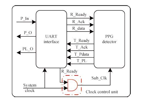
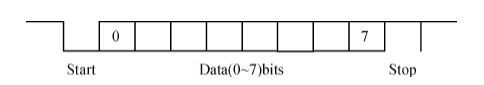
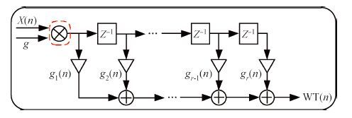
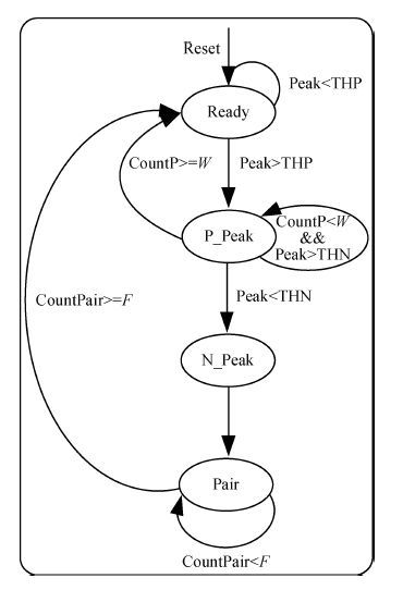
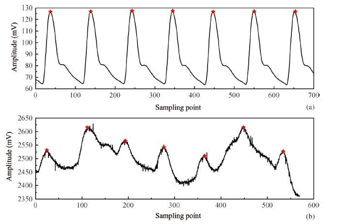
A low power wavelet denoising chip for photoplethysmography (PPG) detection and portable heart rate monitoring is presented. To eliminate noise and improve detection accuracy, Harr wavelet (HWT) is chosen as the processing tool. An optimized finite impulse response structure is proposed to lower the computational complexity of proposed algorithm, which is benefit for reducing the power consumption of proposed chip. The modulus maxima pair location module is design to accurately locate the PPG peaks. A clock control unit is designed to further reduce the power consumption of the proposed chip. Fabricated with the 0.18 μm N-well CMOS 1P6M technology, the power consumption of proposed chip is only 8.12 μ W in 1 V voltage supply. Validated with PPG signals in multiparameter intelligent monitoring in intensive care databases and signals acquired by the wrist photoelectric volume detection front end, the proposed chip can accurately detect PPG signals. The average sensitivity and positive prediction are 99.91% and 100%, respectively.


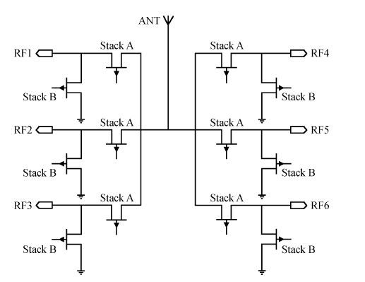
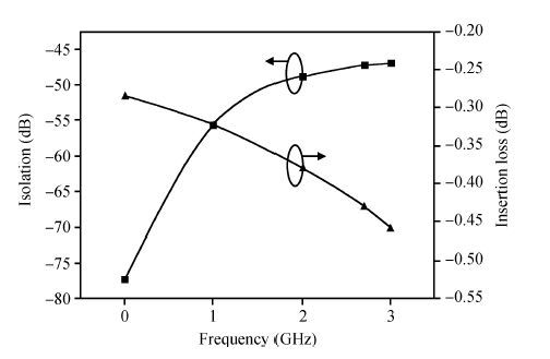
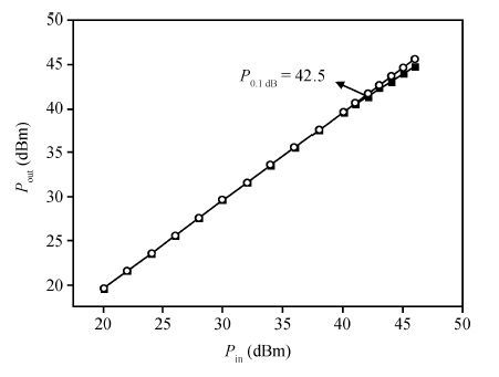
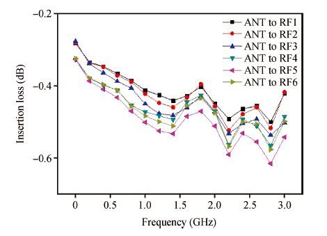
This paper presents the design of single-pole six-throw (SP6T) RF switch with IBM 0.18 μm SOI CMOS technology, which can be widely used in a wireless communication system with its high performance and low cost. The circuit is designed and simulated by using an idea that the total load is divided into six branches and SOI special structures. The insertion loss is less than 0.6 dB, isolation is more than 30 dB, the input power P0.1dB for 0.1 dB compression point is more than 37.5 dBm, IIP3 is more than 70 dBm, the 2nd and the 3rd harmonic compressions are more than 96 dBc, and the control voltage is (+2.46 V, 0, -2.46 V) in the frequency from 0.1 to 2.7 GHz.


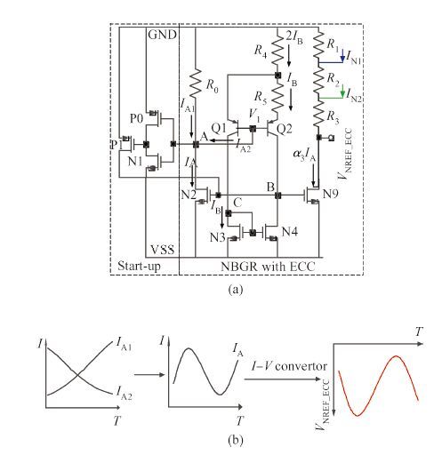
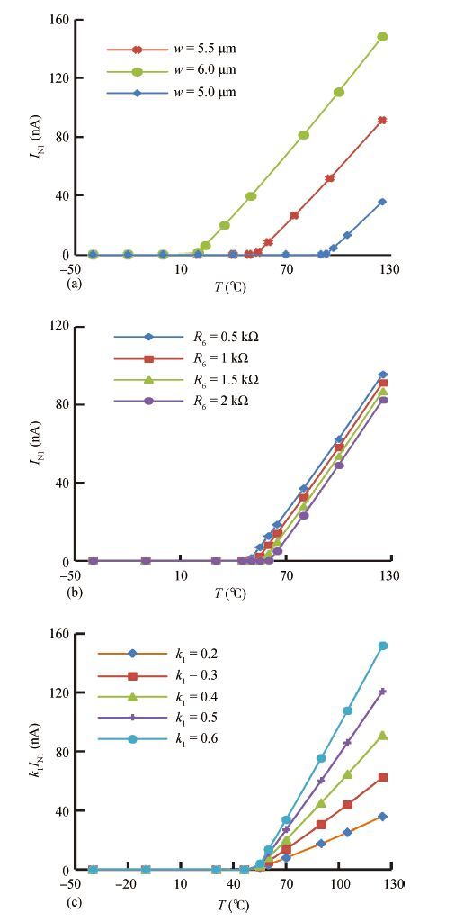
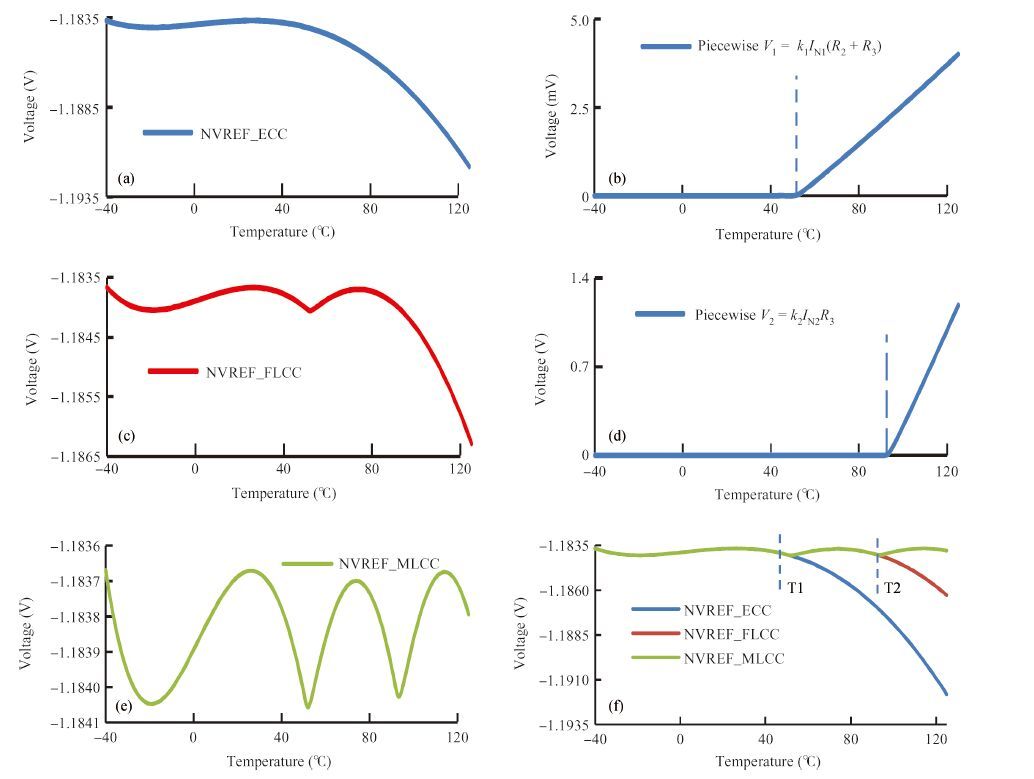
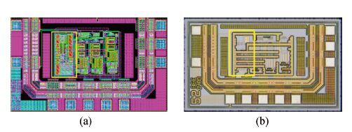
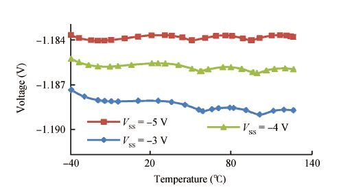
A novel high-order curvature compensation negative voltage bandgap reference (NBGR) based on a novel multilevel compensation technique is introduced. Employing an exponential curvature compensation (ECC) term with many high order terms in itself, in a lower temperature range (TR) and a multilevel curvature compensation (MLCC) term in a higher TR, a flattened and better effect of curvature compensation over the TR of 165 ℃ (-40 to 125 ℃ ) is realised. The MLCC circuit adds two convex curves by using two sub-threshold operated NMOS. The proposed NBGR implemented in the Central Semiconductor Manufacturing Corporation (CSMC) 0.5 μm BCD technology demonstrates an accurate voltage of -1.183 V with a temperature coefficient (TC) as low as 2.45 ppm/℃ over the TR of 165 ℃ at a -5.0 V power supply; the line regulation is 3 mV/V from a -5 to -2 V supply voltage. The active area of the presented NBGR is 370 × 180 μm2.


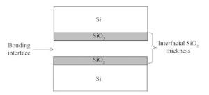
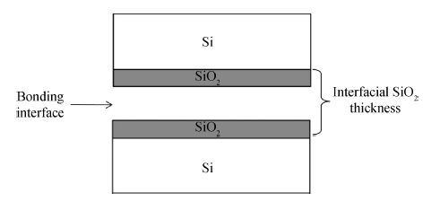
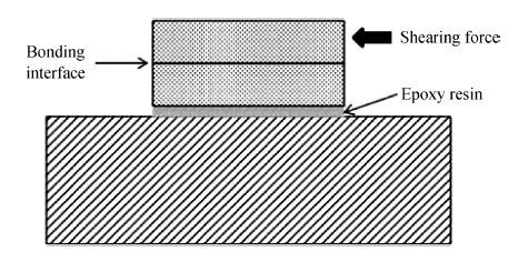
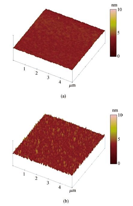
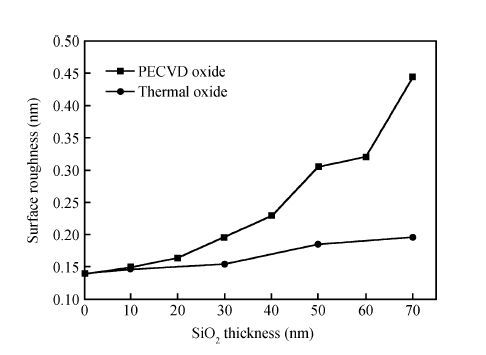
A silicon wafer direct bonding with a thin SiO2 layer at the interface was investigated. An atomic force microscope (AFM) was employed to characterize the surface roughness and a shearing test was carried out to evaluate the bonding strength. Experiments were performed to analyze the relations of surface roughness and bonding strength with the thickness of SiO2 which was grown by thermal oxidation and plasma enhanced chemical vapor deposition (PECVD) respectively. The bonding strength can reach up to 18 MPa for thermal oxidation and 8 MPa for PECVD after a 2-h 400 ℃ annealing. Results indicate that the bonding strength is negatively correlated to the thickness of SiO2 at the interface, which is important in designing the MEMS-based devices and other devices built with wafer direct bonding.