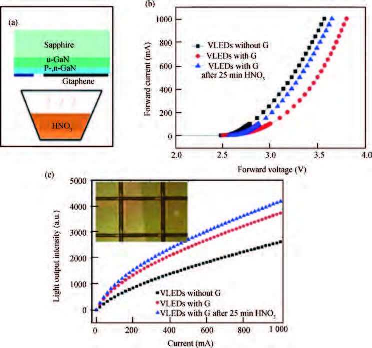
Due to their low power consumption, long lifetime and high efficiency, nitrides based white light-emitting-diodes (LEDs) have long been considered to be a promising technology for next generation illumination. In this work, we provide a brief review of the development of GaN based LEDs. Some pioneering and significant experiment results of our group and the overview of the recent progress in this field are presented. We hope it can provide some meaningful information for the development of high efficiency GaN based LEDs and solid-state-lighting.
Issue Browser
Volume 37, Issue 6,
Jun 2016


J. Semicond.
2016, 37(6): 063001 doi: 10.1088/1674-4926/37/6/063001
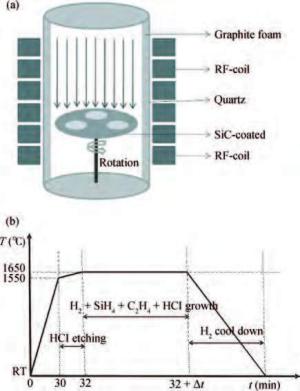
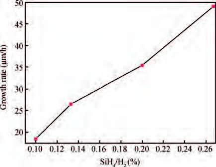
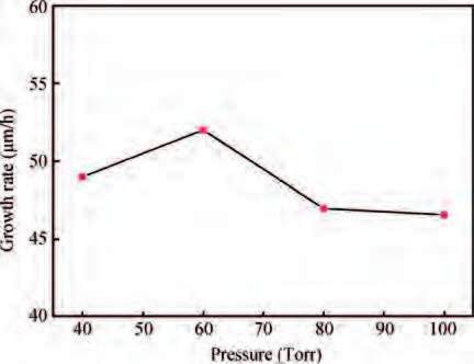
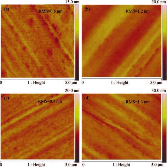
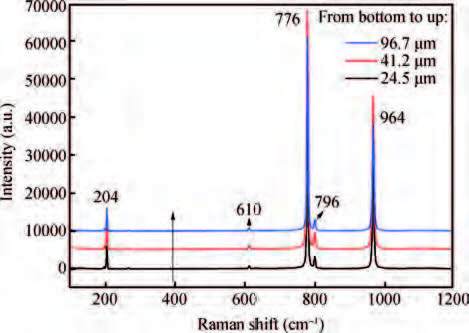
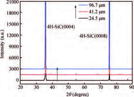
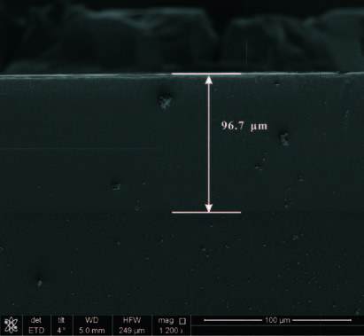
Chloride-based fast homoepitaxial growth of 4H-SiC epilayers was performed on 4° off-axis 4H-SiC substrates in a home-made vertical hot-wall chemical vapor deposition (CVD) system using H2-SiH4-C2H4-HCl. The effect of the SiH4/H2 ratio and reactor pressure on the growth rate of 4H-SiC epilayers has been studied successively. The growth rate increase in proportion to the SiH4/H2 ratio and the influence mechanism of chlorine has been investigated. With the reactor pressure increasing from 40 to 100 Torr, the growth rate increased to 52 μm/h and then decreased to 47 μm/h, which is due to the joint effect of H2 and HCl etching as well as the formation of Si clusters at higher reactor pressure. The surface root mean square (RMS) roughness keeps around 1 nm with the growth rate increasing to 49 μm/h. The scanning electron microscope (SEM), Raman spectroscopy and X-ray diffraction (XRD) demonstrate that 96.7 μm thick 4H-SiC layers of good uniformity in thickness and doping with high crystal quality can be achieved. These results prove that chloride-based fast epitaxy is an advanced growth technique for 4H-SiC homoepitaxy.
J. Semicond.
2016, 37(6): 063002 doi: 10.1088/1674-4926/37/6/063002

Low dislocation density Ge wafers grown by a vertical gradient freeze (VGF) method used for the fabrication of multi-junction photovoltaic cells (MJC) have been studied by a whole wafer scale measurement of the lattice parameter, X-ray rocking curves, etch pit density (EPD), impurities concentration, minority carrier lifetime and residual stress. Impurity content in the VGF-Ge wafers, including that of B, is quite low although B2O3 encapsulation is used in the growth process. An obvious difference exists across the whole wafer regarding the distribution of etch pit density, lattice parameter, full width at half maximum (FWHM) of the X-ray rocking curve and residual stress measured by Raman spectra. These are in contrast to a reference Ge substrate wafer grown by the Cz method. The influence of the VGF-Ge substrate on the performance of the MJC is analyzed and evaluated by a comparison of the statistical results of cell parameters.
J. Semicond.
2016, 37(6): 063003 doi: 10.1088/1674-4926/37/6/063003

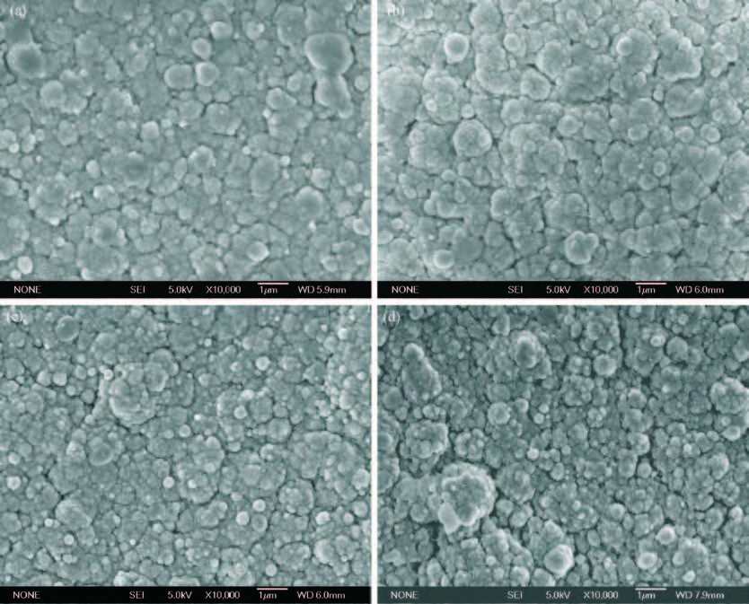
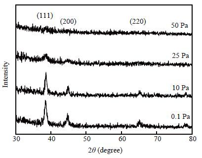
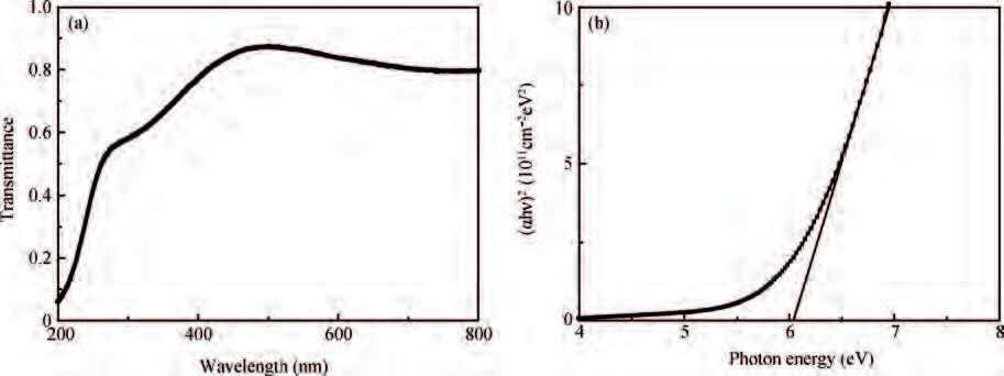
Cubic AlN thin films were obtained on quartz substrate by pulse laser deposition in a nitrogen reactive atmosphere. A Nd-YAG laser with a wavelength of 1064 nm was used as the laser source. In order to study the influence of the process parameters on the deposited AlN film, the experiments were performed at various technique parameters of laser energy density from 70 to 260 J/cm2, substrate temperature from room temperature to 800℃ and nitrogen pressure from 0.1 to 50 Pa. X-ray diffraction, scanning electron microscopy and X-ray photoelectron spectroscopy were applied to characterize the structure and surface morphology of the deposited AlN films. It was found that the structure of AlN films deposited in a vacuum is rocksalt under the condition of substrate temperature 600-800℃, nitrogen pressure 10-0.1 Pa and a moderate laser energy density (190 J/cm2). The high quality AlN film exhibited good optical property.


J. Semicond.
2016, 37(6): 063004 doi: 10.1088/1674-4926/37/6/063004

As the era of nanoelectronics is dawning, CNT (carbon nanotube), a one-dimensional nano material with outstanding properties and performances, has aroused wide attention. In order to study its optical and electrical properties, this paper has researched the influence of tension-twisting deformation, defects, and mixed type on the electronic structure and optical properties of the armchair carbon nanotube superlattices doped cyclic alternately with B and N by using the first-principle method. Our findings show that if tension-twisting deformation is conducted, then the geometric structure, bond length, binding energy, band gap and optical properties of B, N doped carbon nanotube superlattices with defects and mixed type will be influenced. As the degree of exerted tension-twisting deformation increases, B, N doped carbon nanotube superlattices become less stable, and B, N doped carbon nanotube superlattices with defects are more stable than that with exerted tension-twisting deformations. Proper tension-twisting deformation can adjust the energy gap of the system; defects can only reduce the energy gap, enhancing the system metallicity; while the mixed type of 5% tension, twisting angle of 15° and atomic defects will significantly increase the energy gap of the system. From the perspective of optical properties, doped carbon nanotubes may transform the system from metallicity into semi-conductivity.


J. Semicond.
2016, 37(6): 064001 doi: 10.1088/1674-4926/37/6/064001

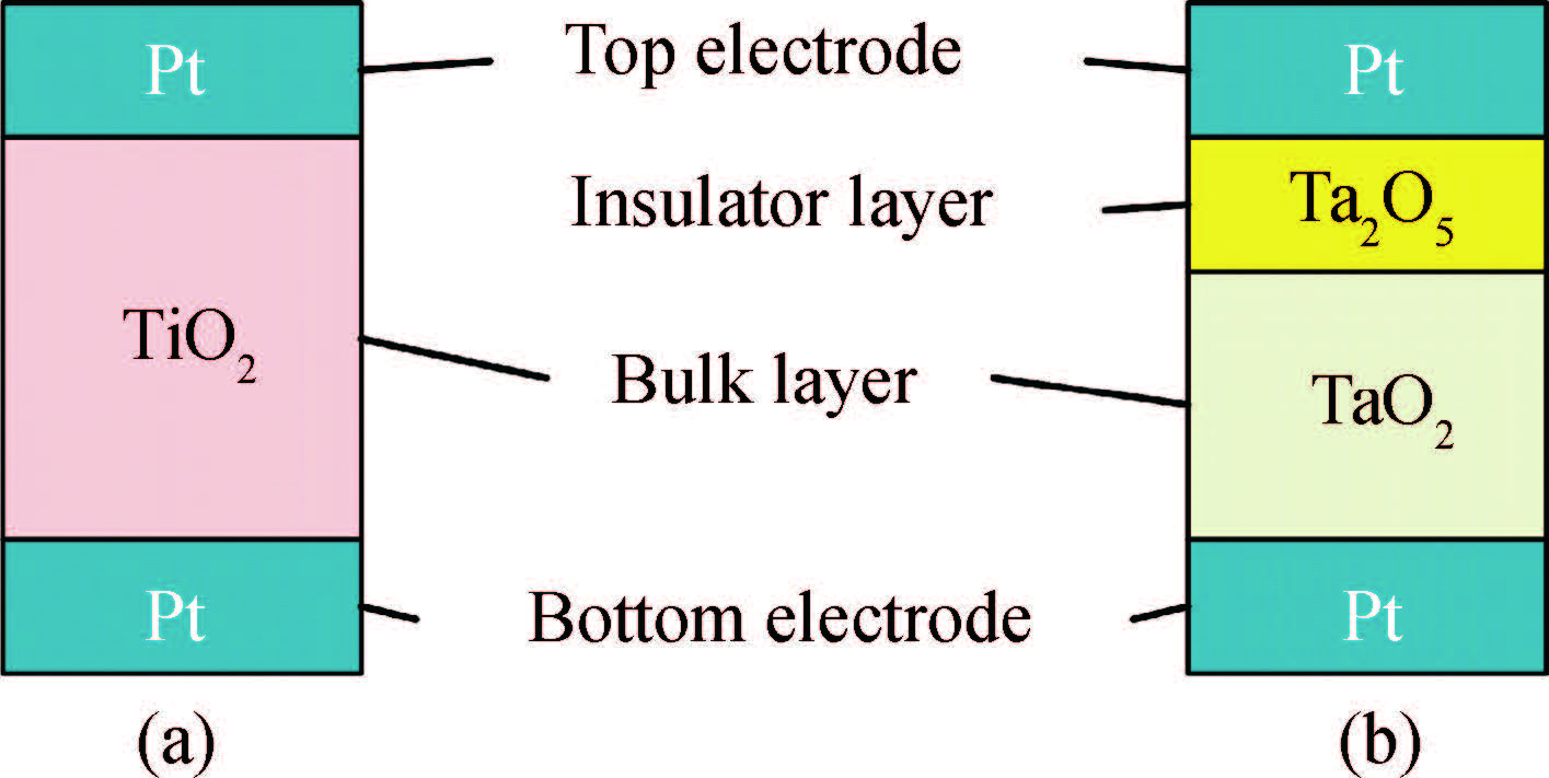
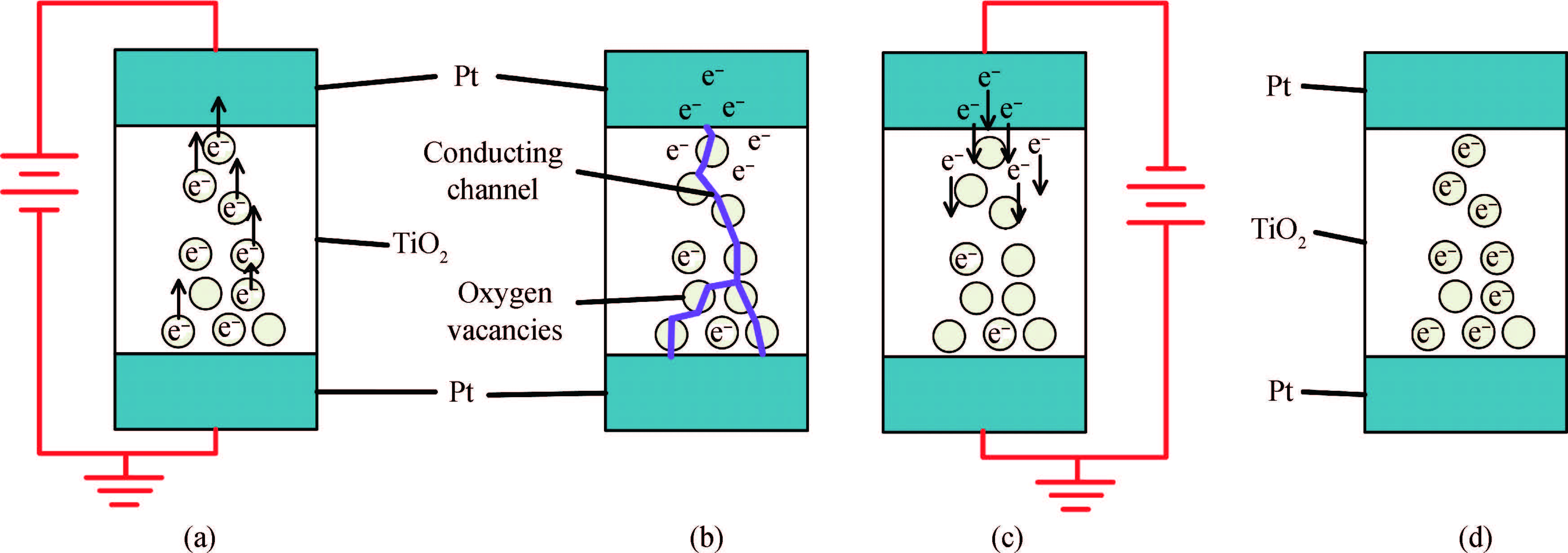
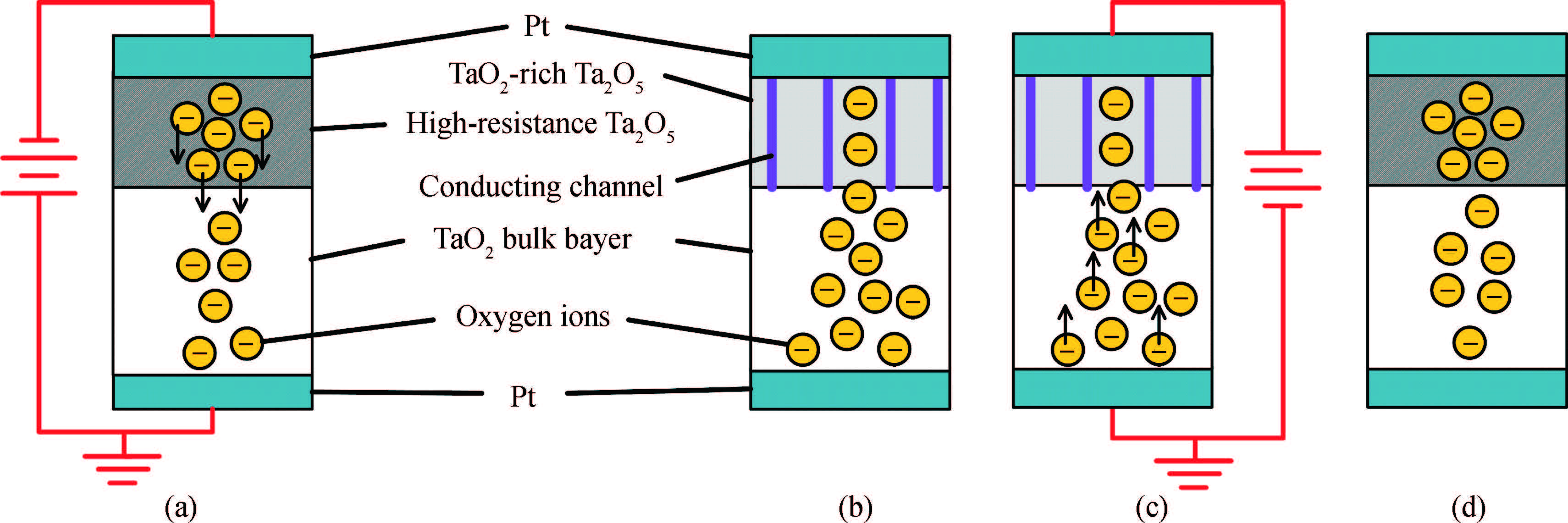
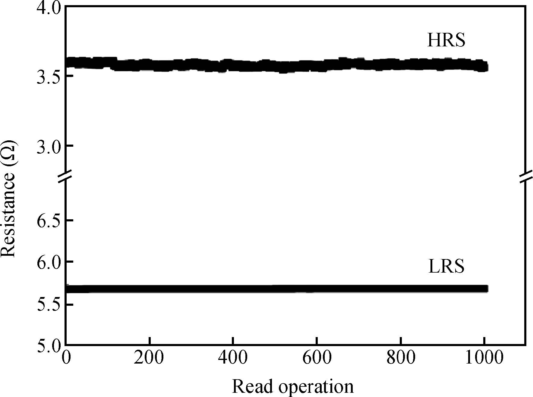
Nonvolatile memories have emerged in recent years and have become a leading candidate towards replacing dynamic and static random-access memory devices. In this article, the performances of TiO2 and TaO2 nonvolatile memristive devices were compared and the factors that make TaO2 memristive devices better than TiO2 memristive devices were studied. TaO2 memristive devices have shown better endurance performances (108 times more switching cycles) and faster switching speed (5 times) than TiO2 memristive devices. Electroforming of TaO2 memristive devices requires~4.5 times less energy than TiO2 memristive devices of a similar size. The retention period of TaO2 memristive devices is expected to exceed 10 years with sufficient experimental evidence. In addition to comparing device performances, this article also explains the differences in physical device structure, switching mechanism, and resistance switching performances of TiO2 and TaO2 memristive devices. This article summarizes the reasons that give TaO2 memristive devices the advantage over TiO2 memristive devices, in terms of electroformation, switching speed, and endurance.
J. Semicond.
2016, 37(6): 064002 doi: 10.1088/1674-4926/37/6/064002
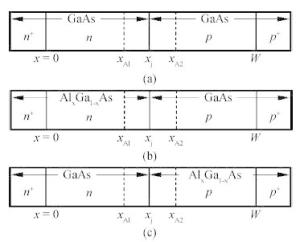
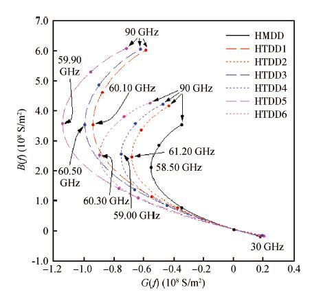
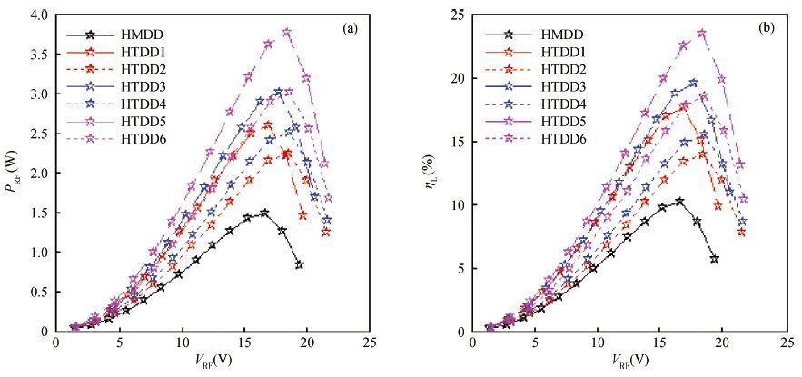
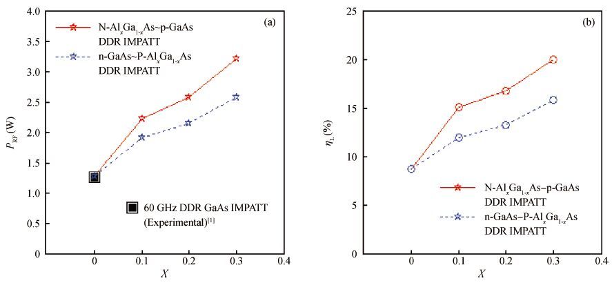
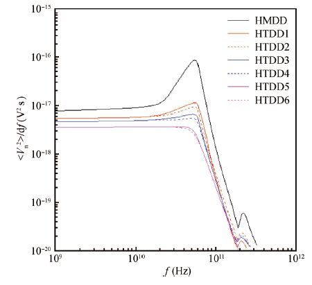
Simulation studies are carried out on the large signal and noise properties of heterojunction (HT) AlxGa1-xAs/GaAs double drift region (DDR) IMPATT devices at V-band (60 GHz). The dependence of Al mole fraction on the aforementioned properties of the device has been investigated. A full simulation software package has been indigenously developed for this purpose. The large signal simulation is based on a non-sinusoidal voltage excitation model. Three mole fractions of Al and two complementary HT DDR structures for each mole fraction i.e., six DDR structures are considered in this study. The purpose is to discover the most suitable structure and corresponding mole fraction at which high power, high efficiency and low noise are obtained from the device. The noise spectral density and noise measure of all six HT DDR structures are obtained from a noise model and simulation method. Similar studies are carried out on homojunction (HM) DDR GaAs IMPATTs at 60 GHz to compare their RF properties with those of HT DDR devices. The results show that the HT DDR device based on N-AlxGa1-xAs/p-GaAs with 30% mole fraction of Al is the best one so far as large signal power output, DC to RF conversion efficiency and noise level are concerned.


J. Semicond.
2016, 37(6): 064003 doi: 10.1088/1674-4926/37/6/064003

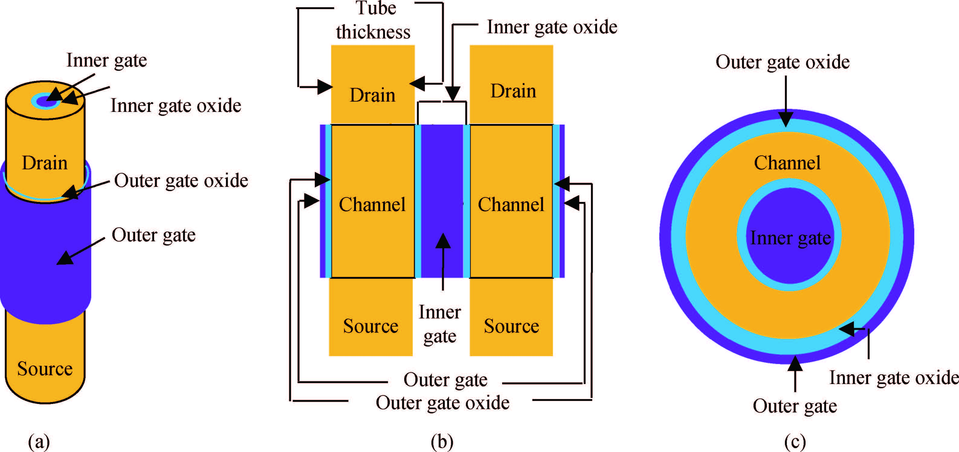
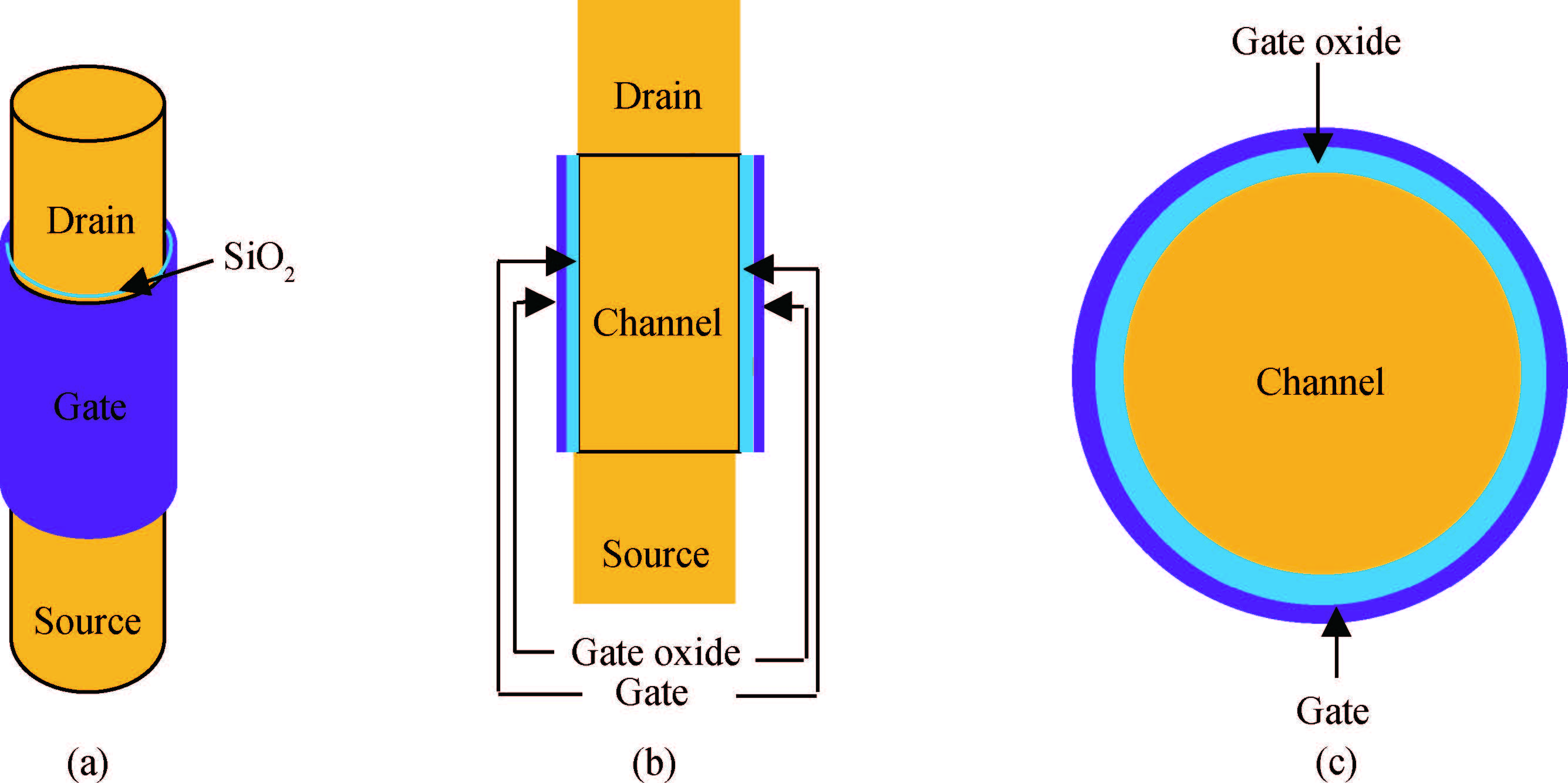
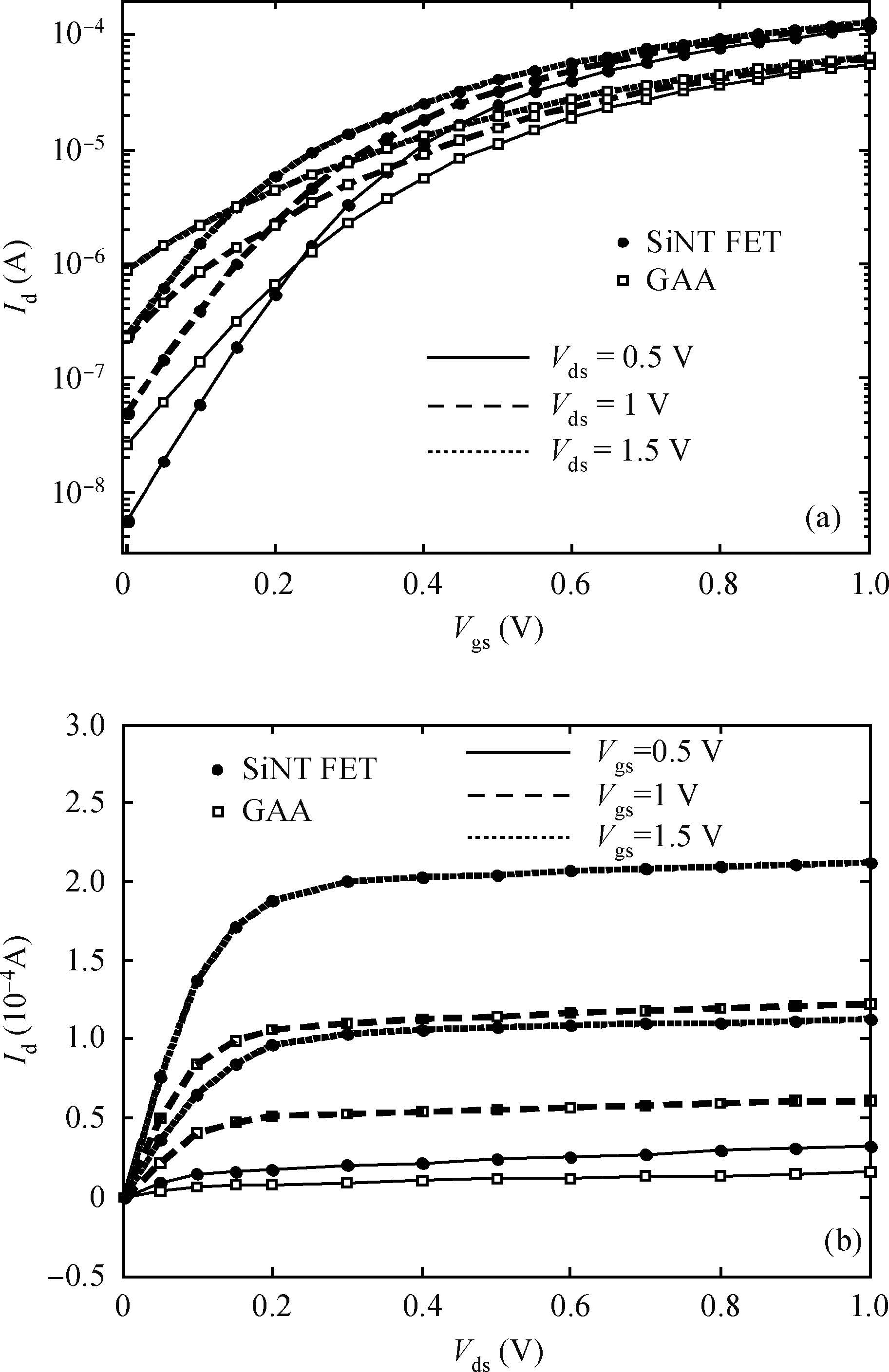
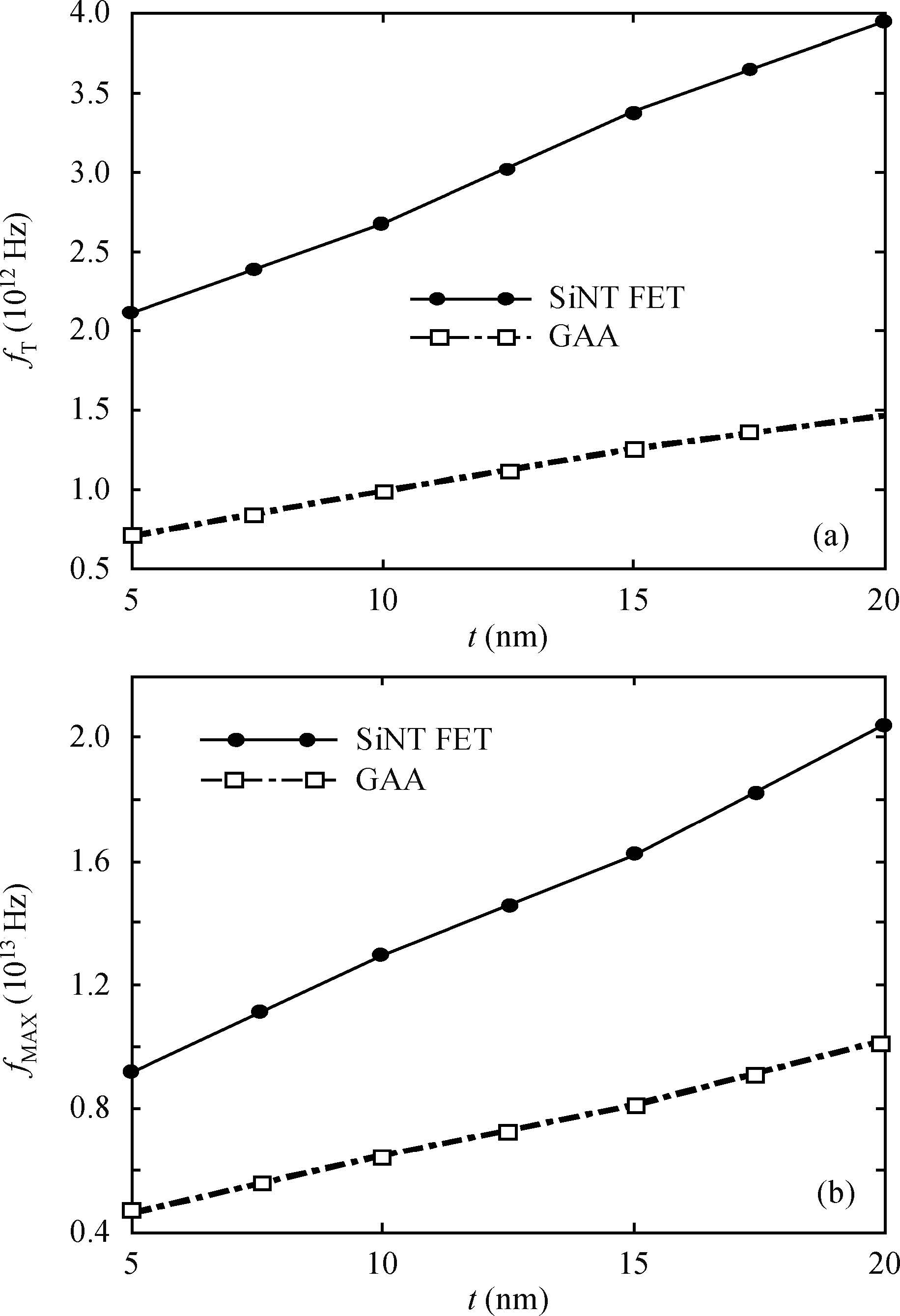
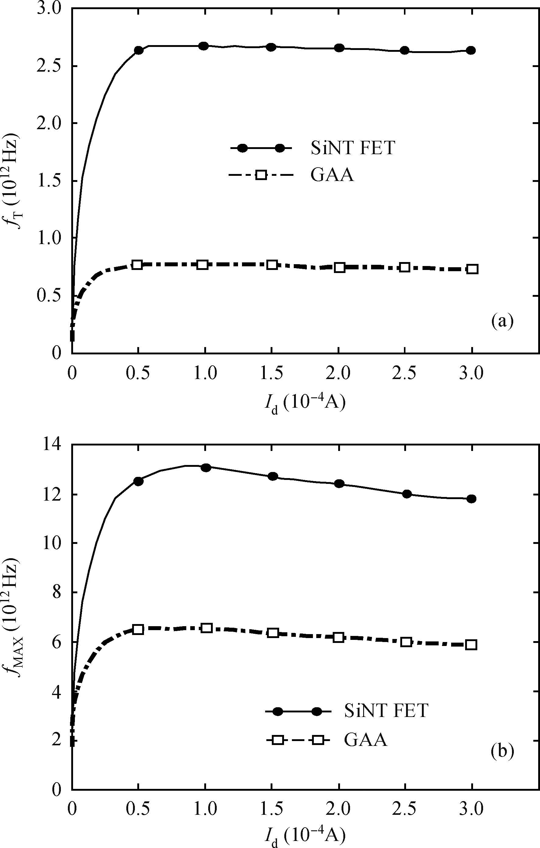
This work presents a comparative study of the influence of various parameters on the analog and RF properties of silicon-nanotube MOSFETs and nanowire-based gate-all-around (GAA) MOSFETs. The important analog and RF performance parameters of SiNT FETs and GAA MOSFETs, namely drain current (Id), transconductance to drain current ratio (gm/Id), Ion/Ioff, the cut-off frequency (fT) and the maximum frequency of oscillation (fMAX) are evaluated with the help of Y- and H-parameters which are obtained from a 3-D device simulator, ATLASTM. It is found that the silicon-nanotube MOSFETs have far more superior analog and RF characteristics (gm/Id, fT and fMAX) compared to the nanowire-based gate-all-around GAA MOSFETs. The silicon-nanotube MOSFET shows an improvement of~2.5 and 3 times in the case of fT and fMAX values respectively compared with the nanowire-based gate-all-around (GAA) MOSFET.


J. Semicond.
2016, 37(6): 064004 doi: 10.1088/1674-4926/37/6/064004
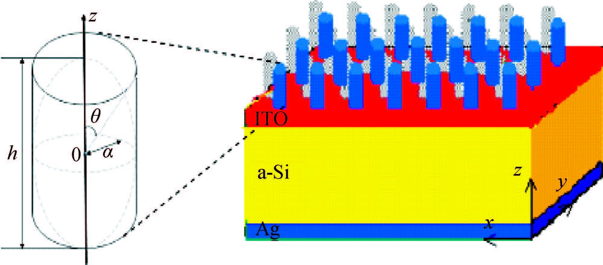
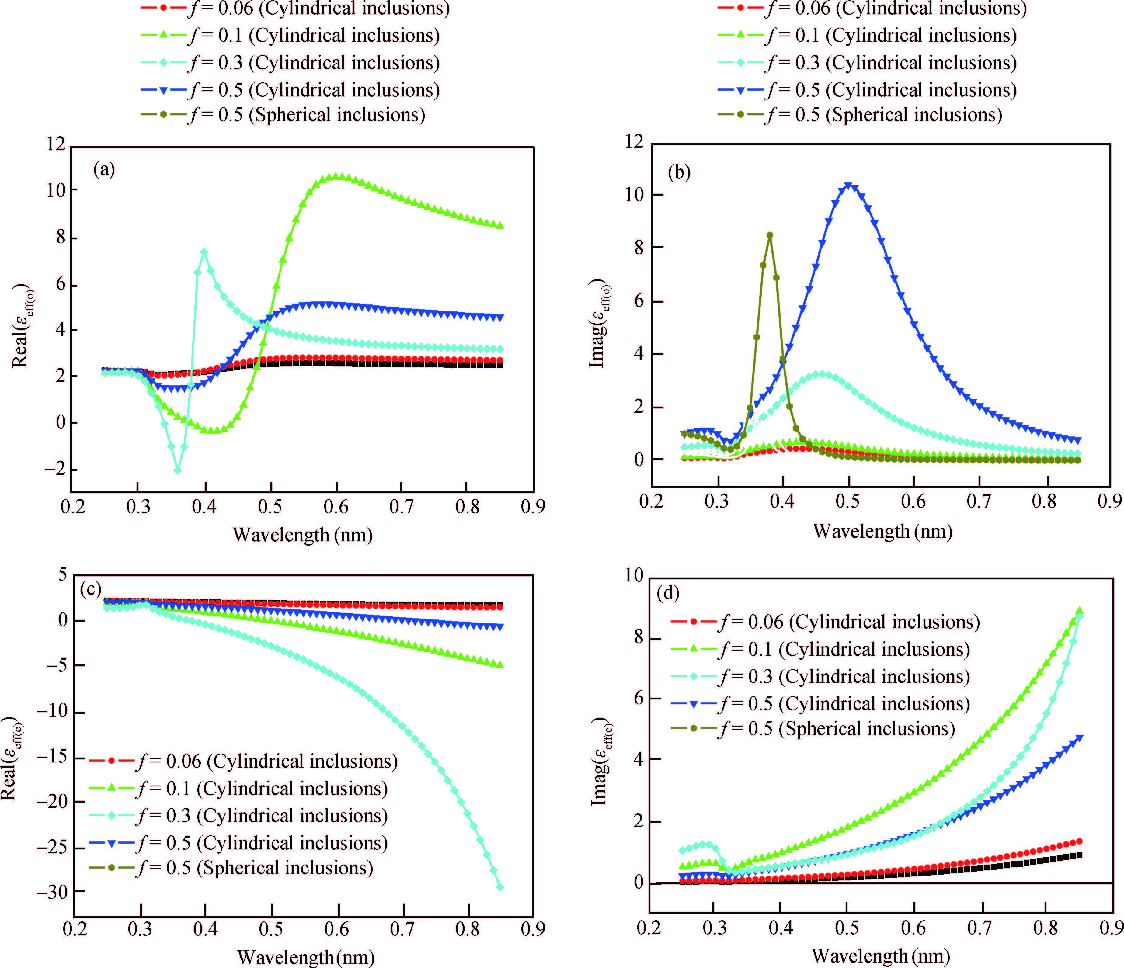
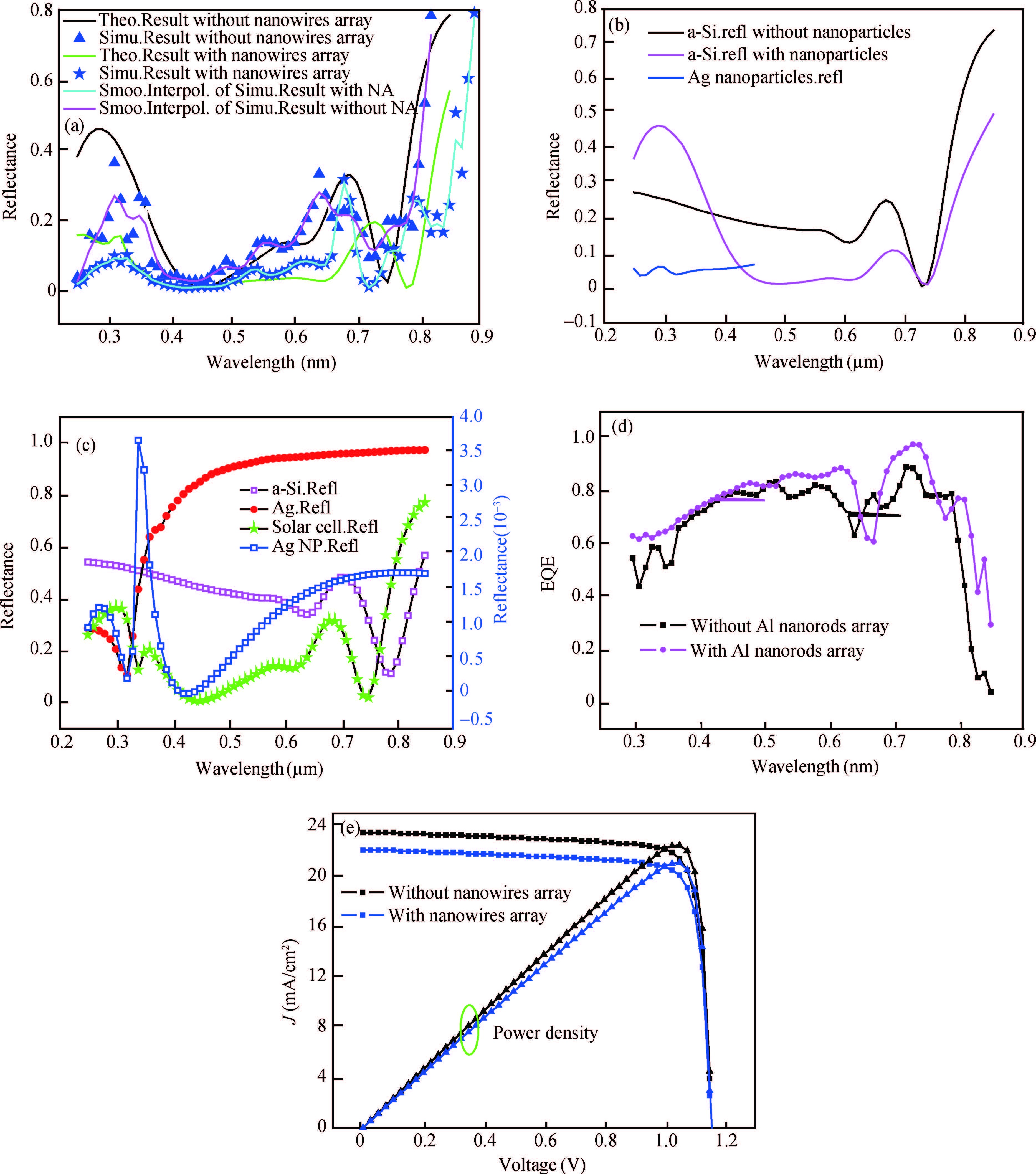
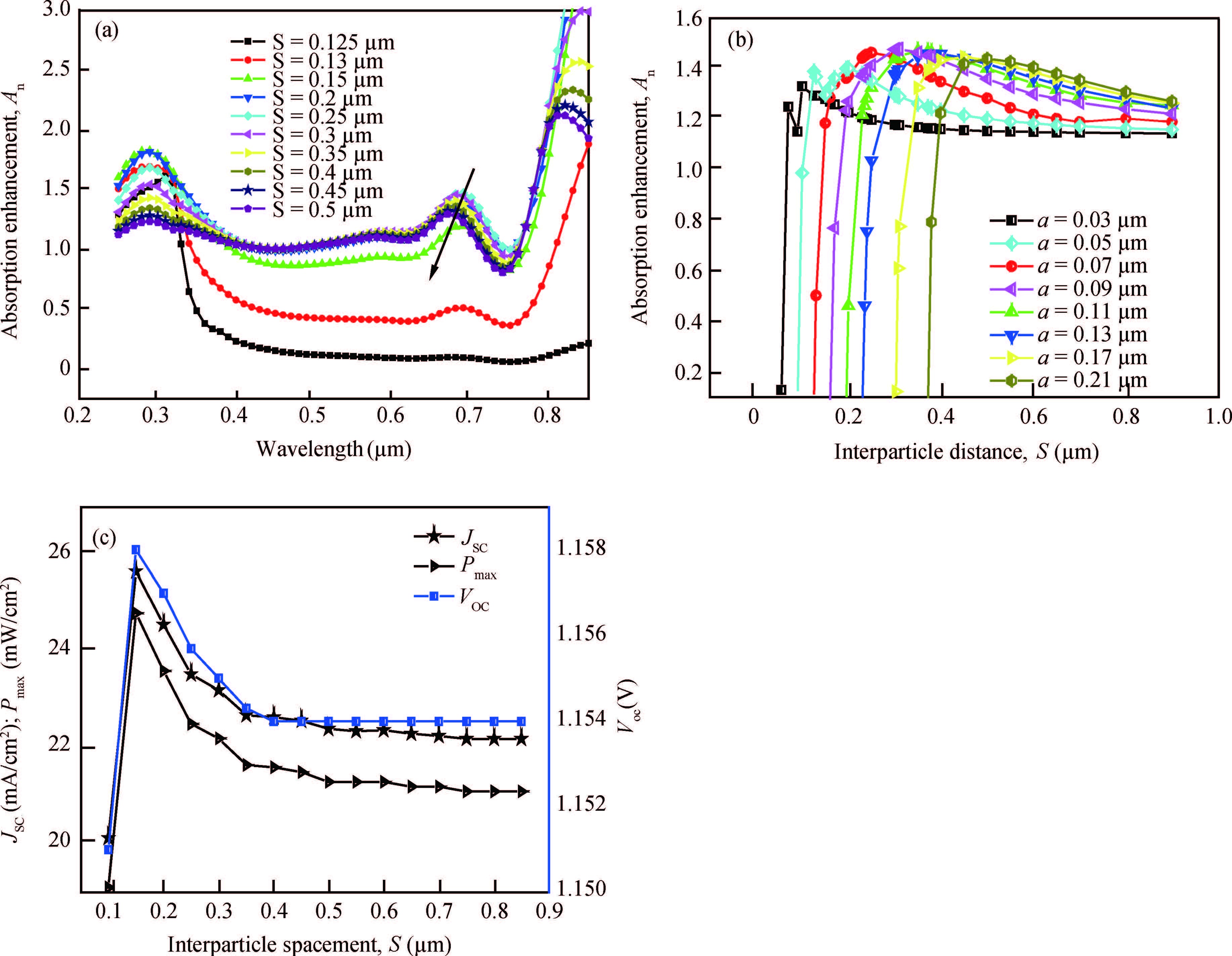
Optical absorption in thin-film solar cells can be improved by using surface plasmons for guiding and confining the light on the nanoscale. We report theoretical and simulation studies of a-Si thin-film solar cells with silver nanocylinders on the surface. We found that surface plasmons increased the cells' spectral response over almost the entire studied solar spectrum. In the ultraviolet range and at wavelengths close to the Si band gap we observed a significant enhancement of the absorption for both thin-film and wafer-based structures. We also performed optimization studies of particle size, inter-particle distance, and dielectric environment, for obtaining maximal absorption within the substrate. A blue-shift of the resonance wavelength with increasing inter-particle distance was observed in the visible range. Cell performance improved at optimal spacing, which strongly depended on the nanoparticle size. Increasing the nanocylinder size was accompanied by the widening of the plasmon resonance band and a red-shift of the plasmon resonance peaks. A weak red-shift and plasmon peak enhancement were observed in the reflectance curve with increasing refractive index of the dielectric spacer.

J. Semicond.
2016, 37(6): 064005 doi: 10.1088/1674-4926/37/6/064005
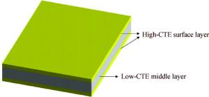
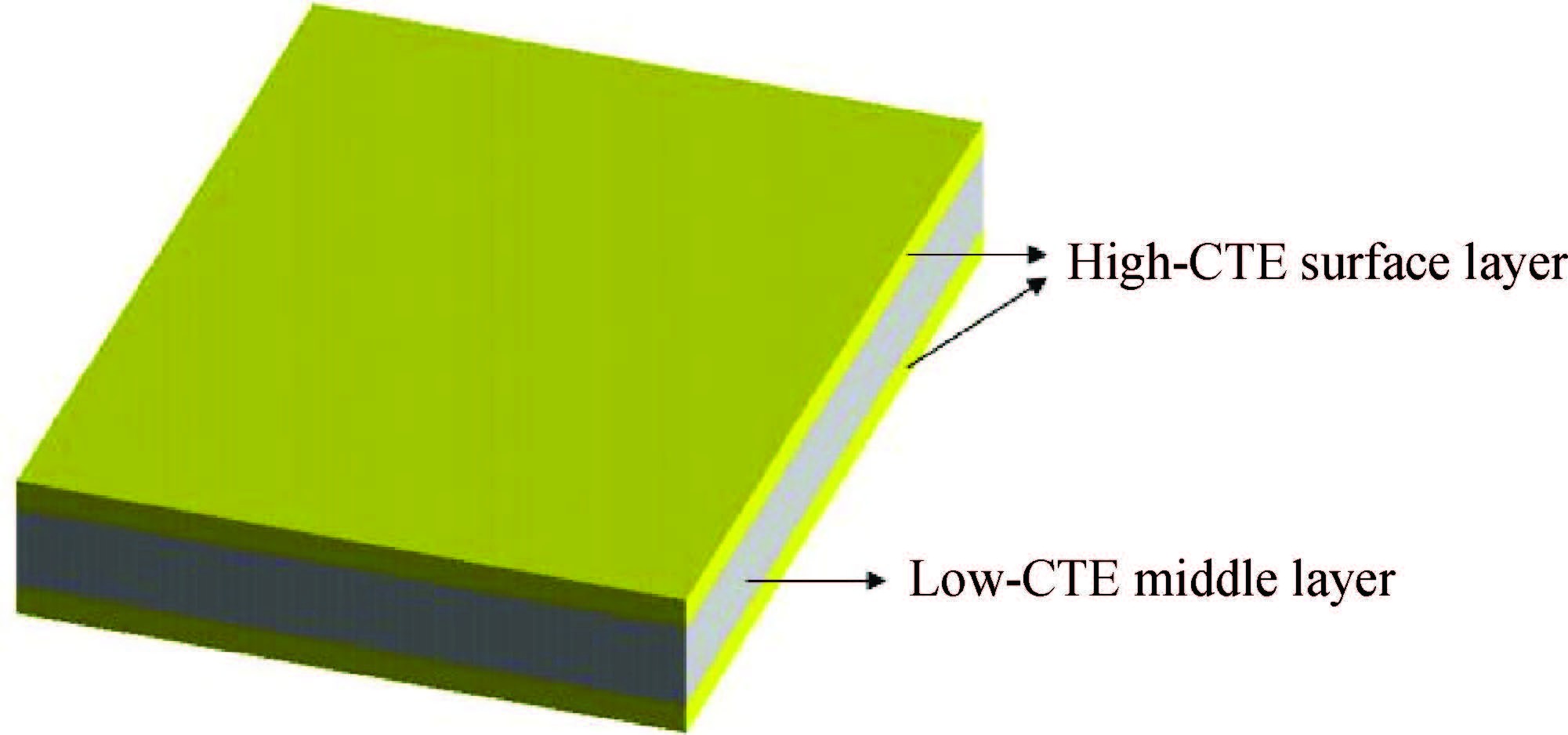
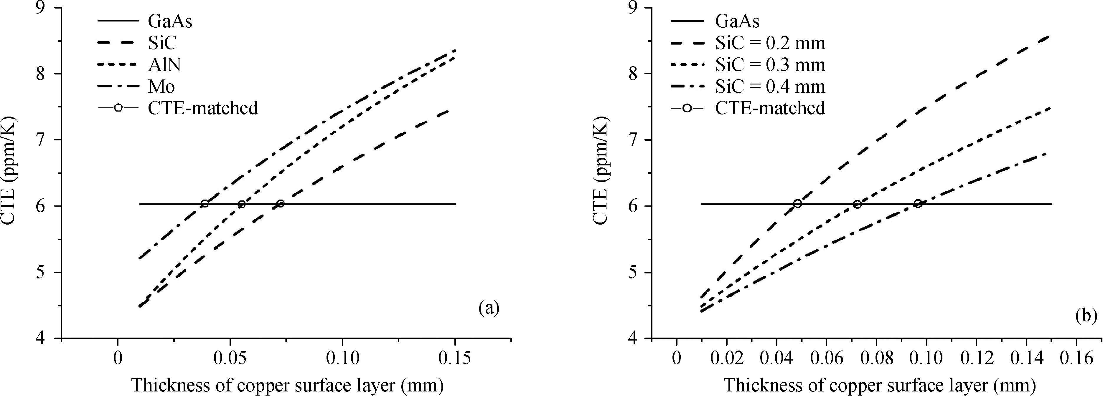
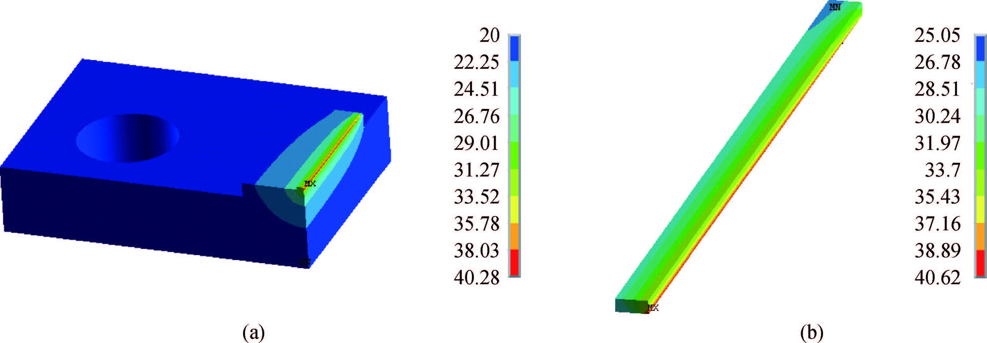
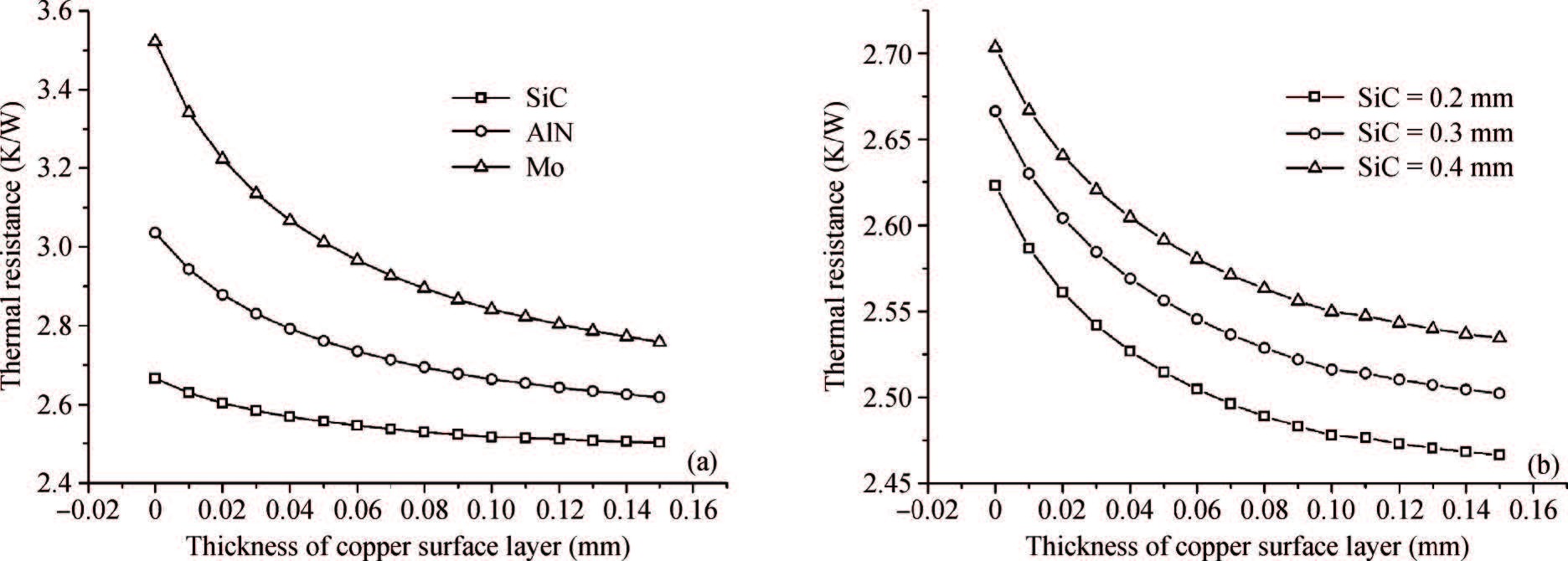
In order to improve the output power and increase the lifetime of laser diodes, expansion-matched submounts were investigated by finite element analysis. The submount was designed as sandwiched structure. By varying the vertical structure and material of the middle layer, the thermal expansion behavior on the mounting surface was simulated to obtain the expansion-matched design. In addition, the thermal performance of laser diodes packaged by different submounts was compared. The numerical results showed that, changing the thickness ratio of surface copper to middle layer will lead the stress and junction temperature to the opposite direction. Thus compromise needs to be made in the design of the vertical structure. In addition, the silicon carbide (SiC) is the most promising material candidate for the middle layer among the materials discussed in this paper. The simulated results were aimed at providing guidance for the optimal design of sandwich-structure submounts.
J. Semicond.
2016, 37(6): 064006 doi: 10.1088/1674-4926/37/6/064006
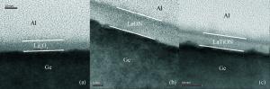
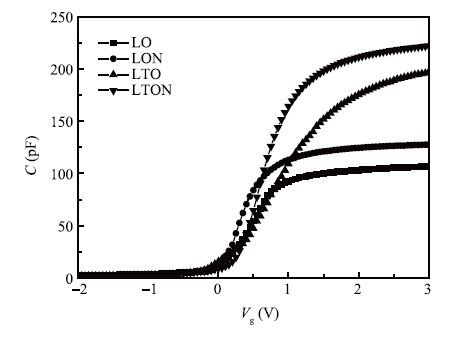
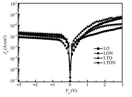
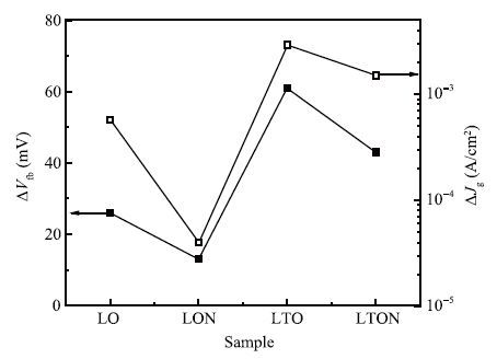
LaON, LaTiO and LaTiON films are deposited as gate dielectrics by incorporating N or/and Ti into La2O3 using the sputtering method to fabricate Ge MOS capacitors, and the electrical properties of the devices are carefully examined. LaON/Ge capacitors exhibit the best interface quality, gate leakage property and device reliability, but a smaller k value (14.9). LaTiO/Ge capacitors exhibit a higher k value (22.7), but a deteriorated interface quality, gate leakage property and device reliability. LaTiON/Ge capacitors exhibit the highest k value (24.6), and a relatively better interface quality (3.1×10¹¹ eV-1cm-2), gate leakage property (3.6×10⁻³ A/cm2 at Vg=1 V+Vfb) and device reliability. Therefore, LaTiON is more suitable for high performance Ge MOS devices as a gate dielectric than LaON and LaTiO materials.

J. Semicond.
2016, 37(6): 064007 doi: 10.1088/1674-4926/37/6/064007

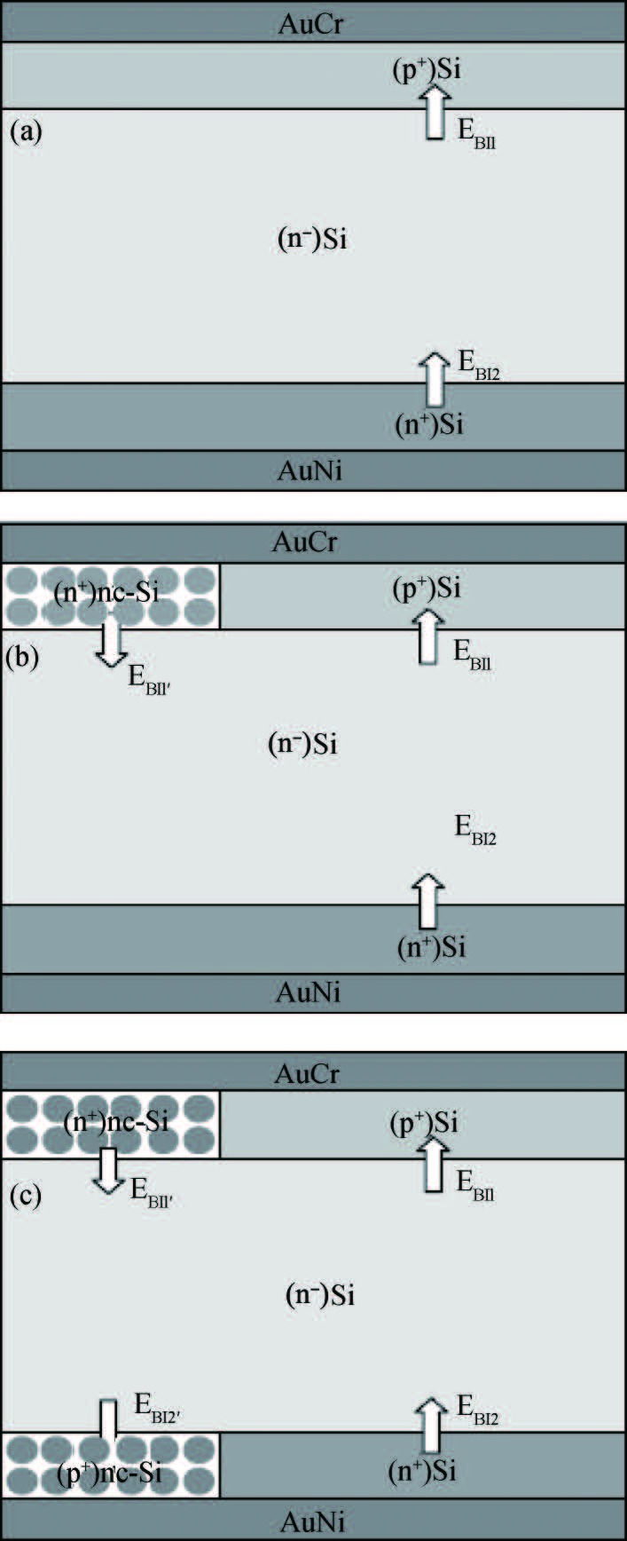
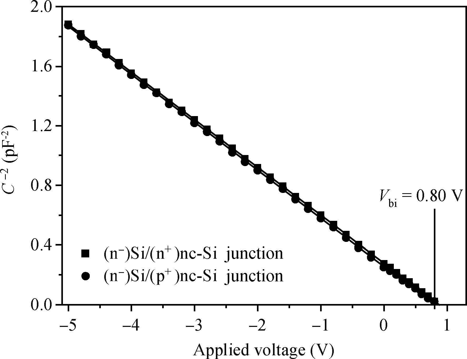
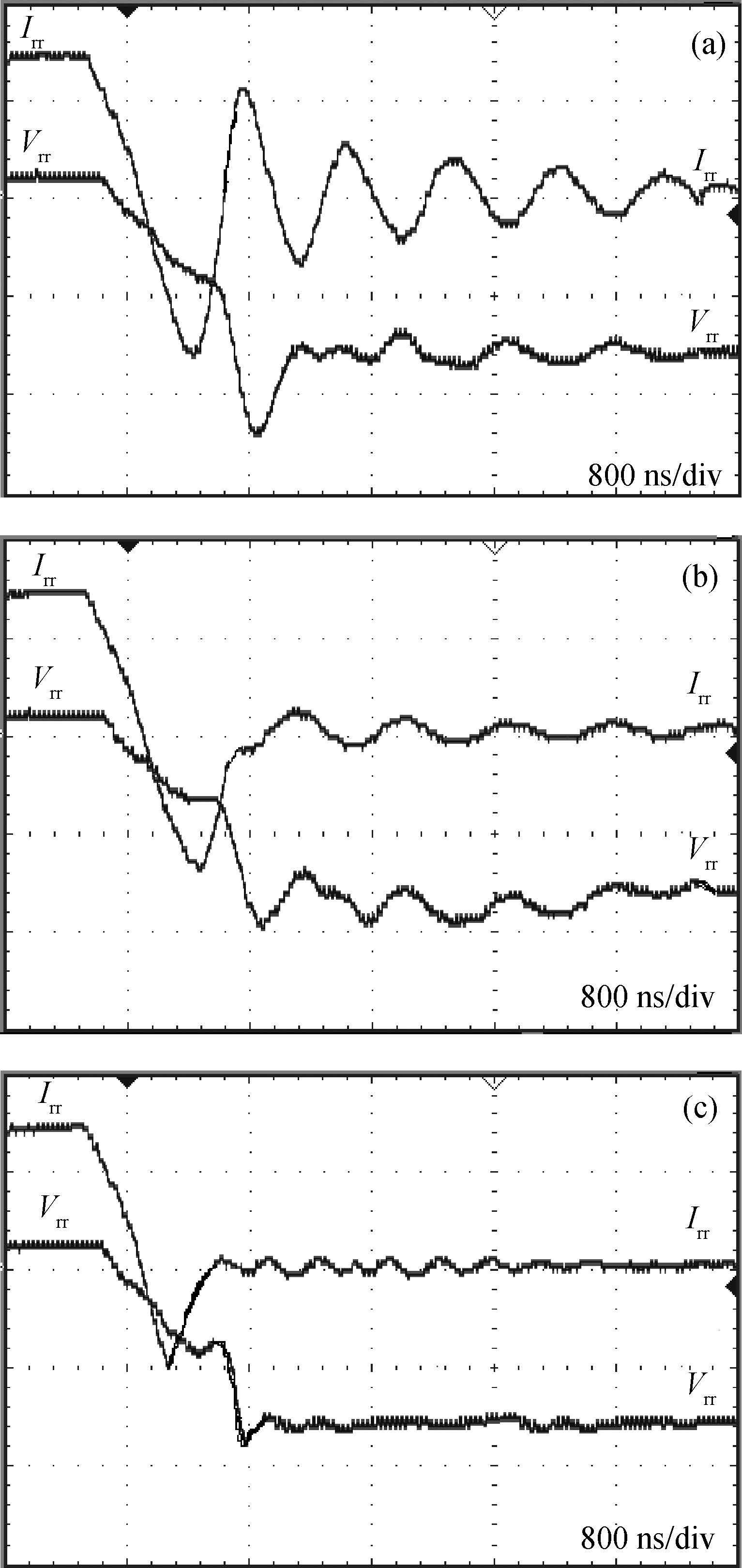
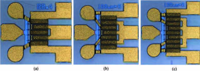
Using p+-type crystalline Si with n+-type nanocrystalline Si (nc-Si) and n+-type crystalline Si with p+-type nc-Si mosaic structures as electrodes, a type of power diode was prepared with epitaxial technique and plasma-enhanced chemical vapor deposition (PECVD) method. Firstly, the basic p+-n--n+-type Si diode was fabricated by epitaxially growing p+- and n+-type layers on two sides of a lightly doped n--type Si wafer respectively. Secondly, heavily phosphorus-doped Si film was deposited with PECVD on the lithography mask etched p+-type Si side of the basic device to form a component with mosaic anode. Thirdly, heavily boron-doped Si film was deposited on the etched n+-type Si side of the second device to form a diode with mosaic anode and mosaic cathode. The images of high resolution transmission electronic microscope and patterns of X-ray diffraction reveal nanocrystallization in the phosphorus- and boron-deposited films. Electrical measurements such as capacitance-voltage relation, current-voltage feature and reverse recovery waveform were carried out to clarify the performance of prepared devices. The important roles of (n-)Si/(p+)nc-Si and (n-)Si/(n+)nc-Si junctions in the static and dynamic conduction processes in operating diodes were investigated. The performance of mosaic devices was compared to that of a basic one.


J. Semicond.
2016, 37(6): 064008 doi: 10.1088/1674-4926/37/6/064008

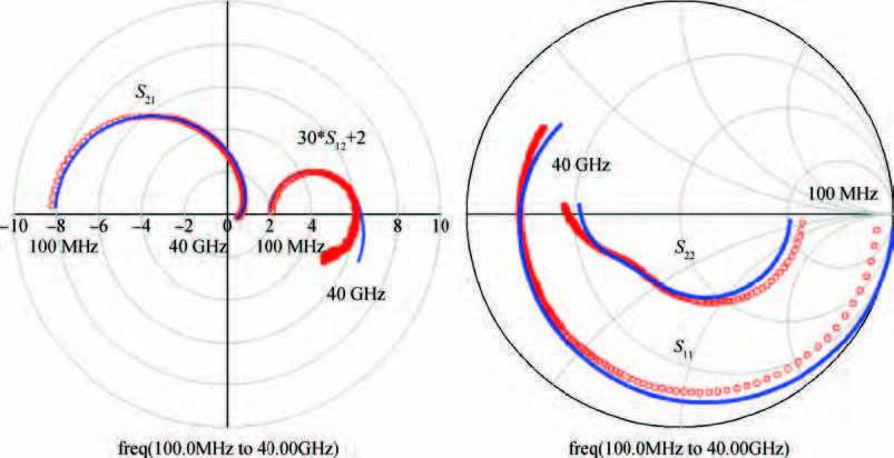
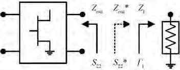
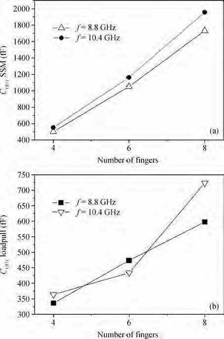
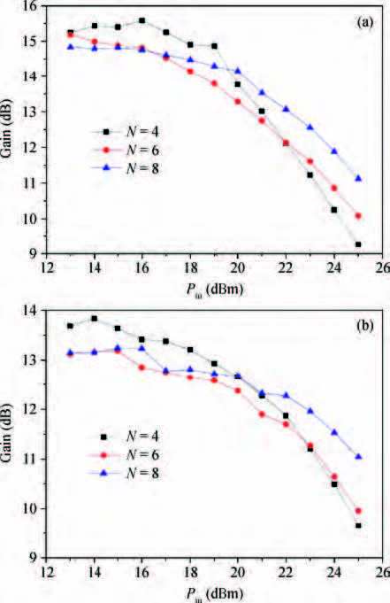
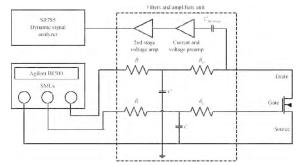
This paper investigates load-pull measurement of AlGaN/GaN high electron mobility transistors (HEMTs) at different numbers of gate fingers. Scalable small-signal models are extracted to analyze the relationship between each model's parameters and the number of device's gate fingers. The simulated S-parameters from the small-signal models are compared with the reflection coefficients measured from the load-pull measurement system at X-band frequencies of 8.8 and 10.4 GHz. The dependency between the number of device's gate fingers and load-pull characterization is presented.

J. Semicond.
2016, 37(6): 064009 doi: 10.1088/1674-4926/37/6/064009

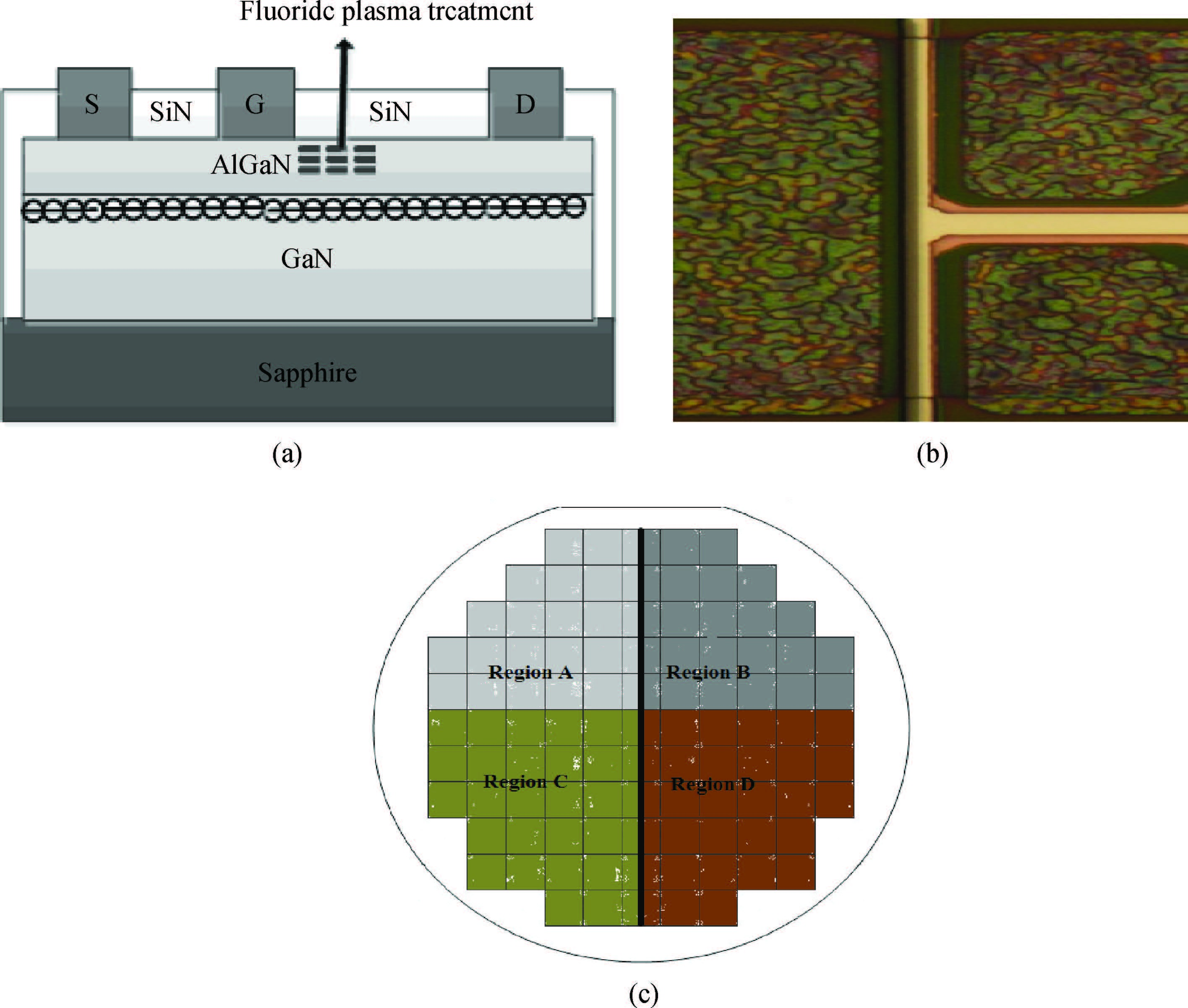
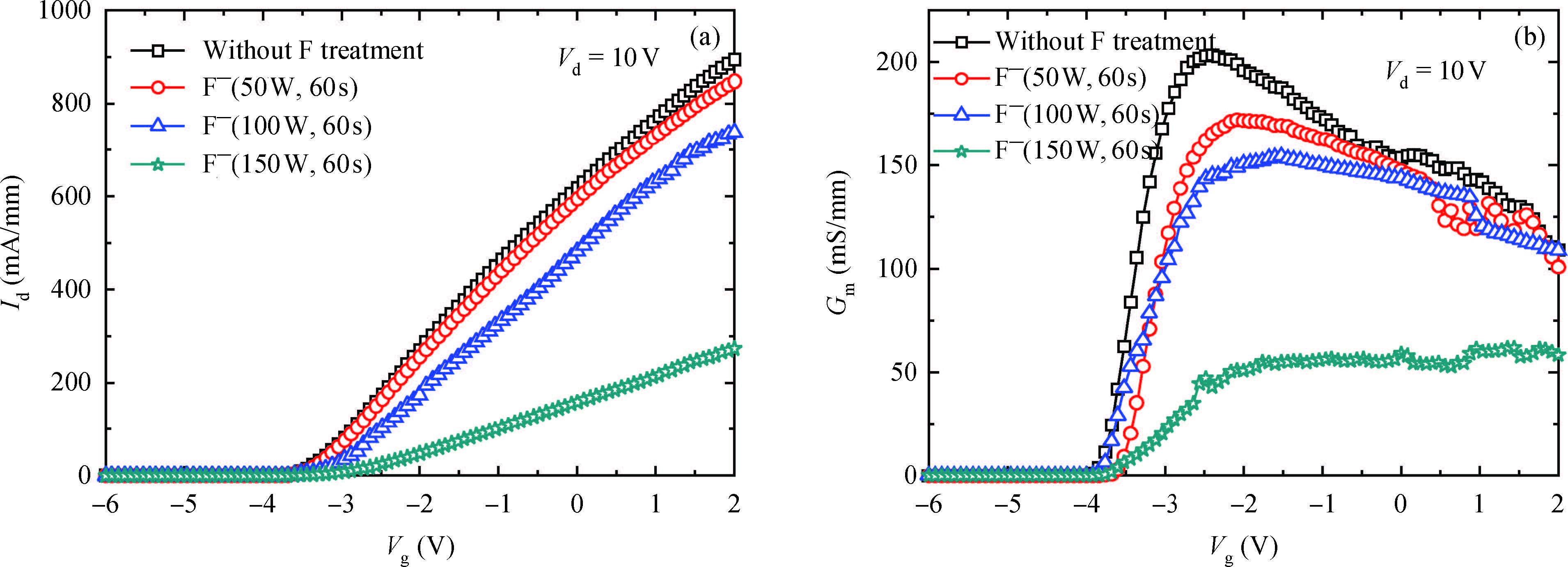
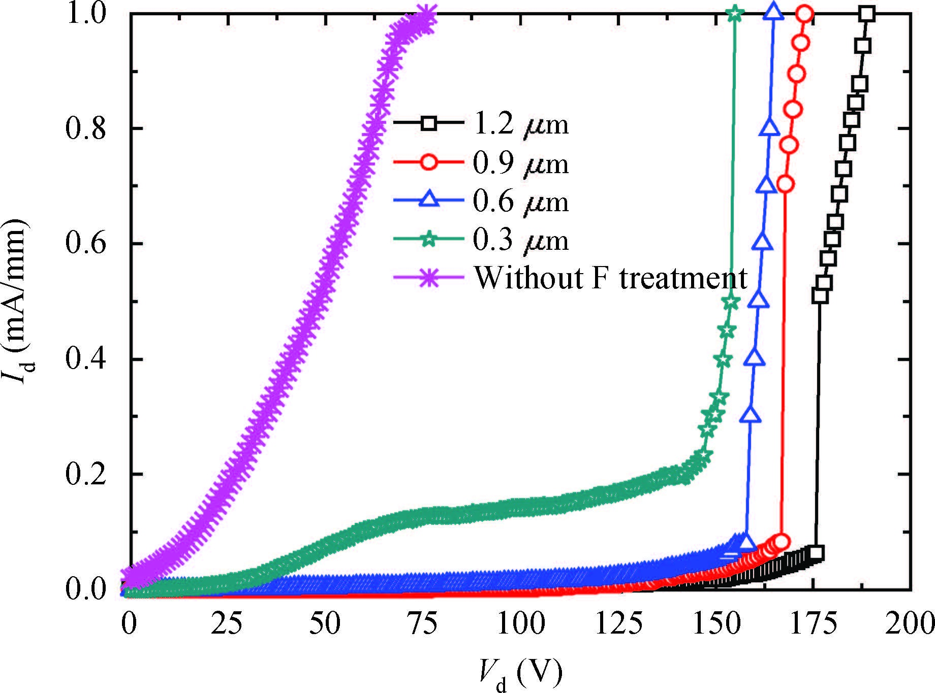
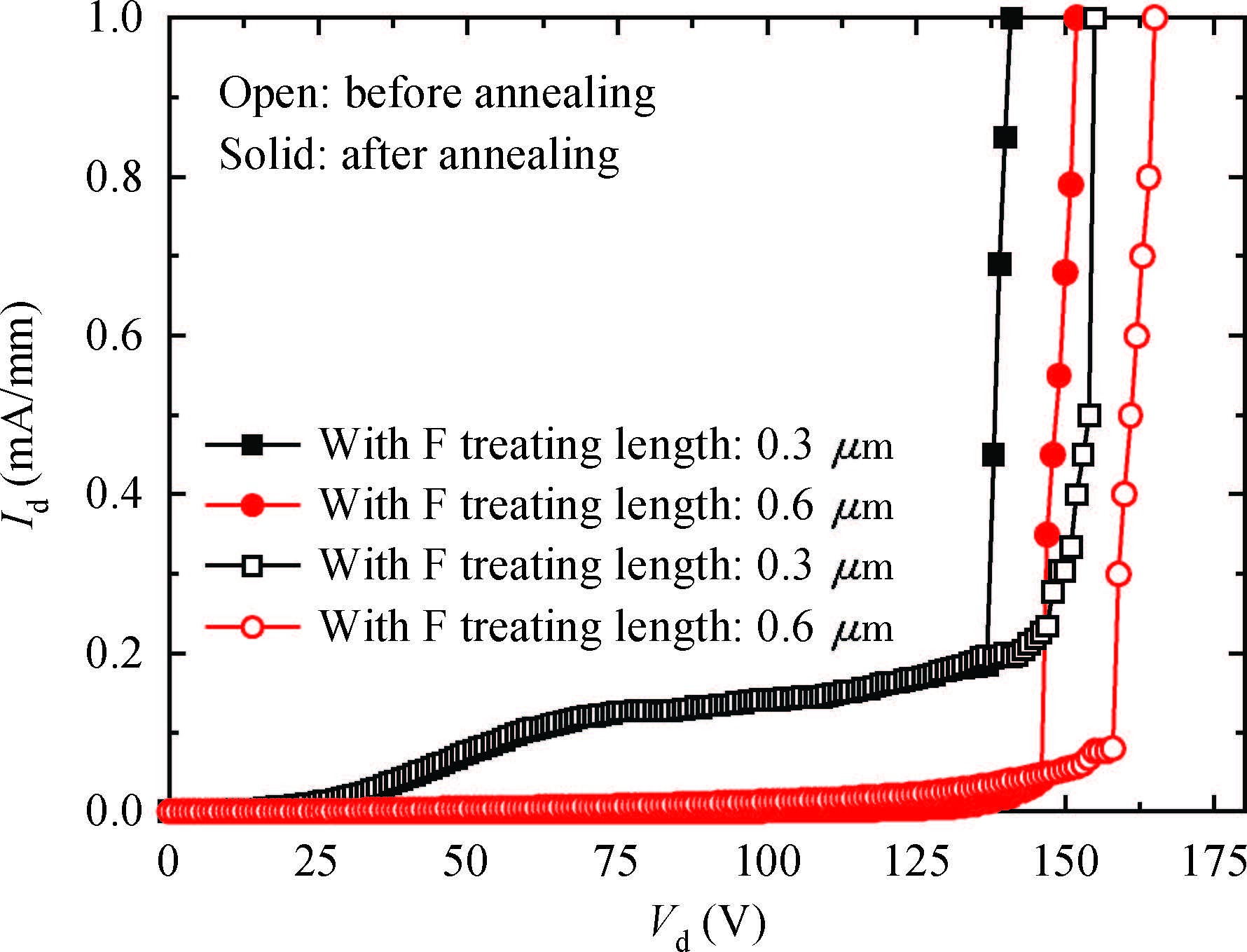
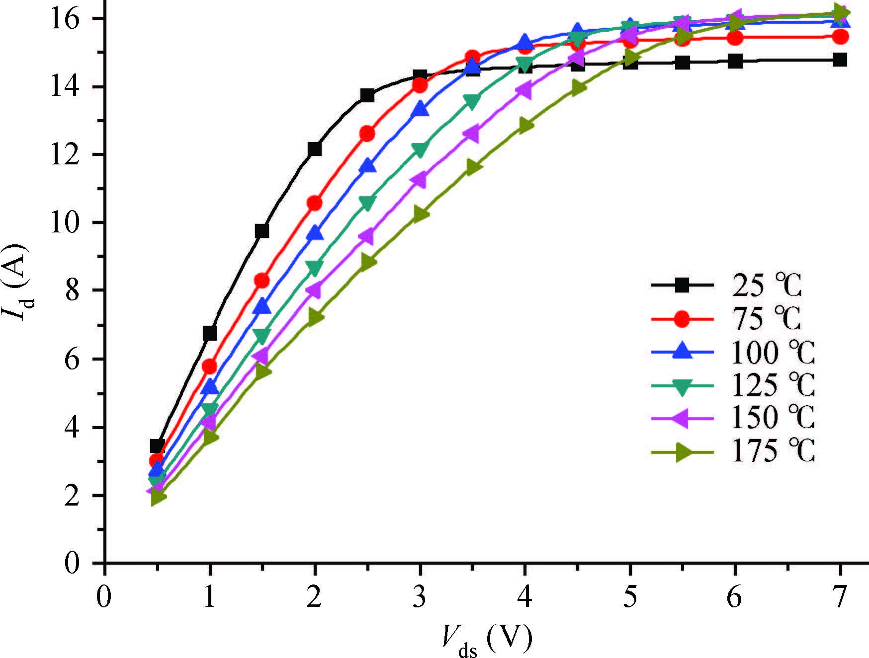
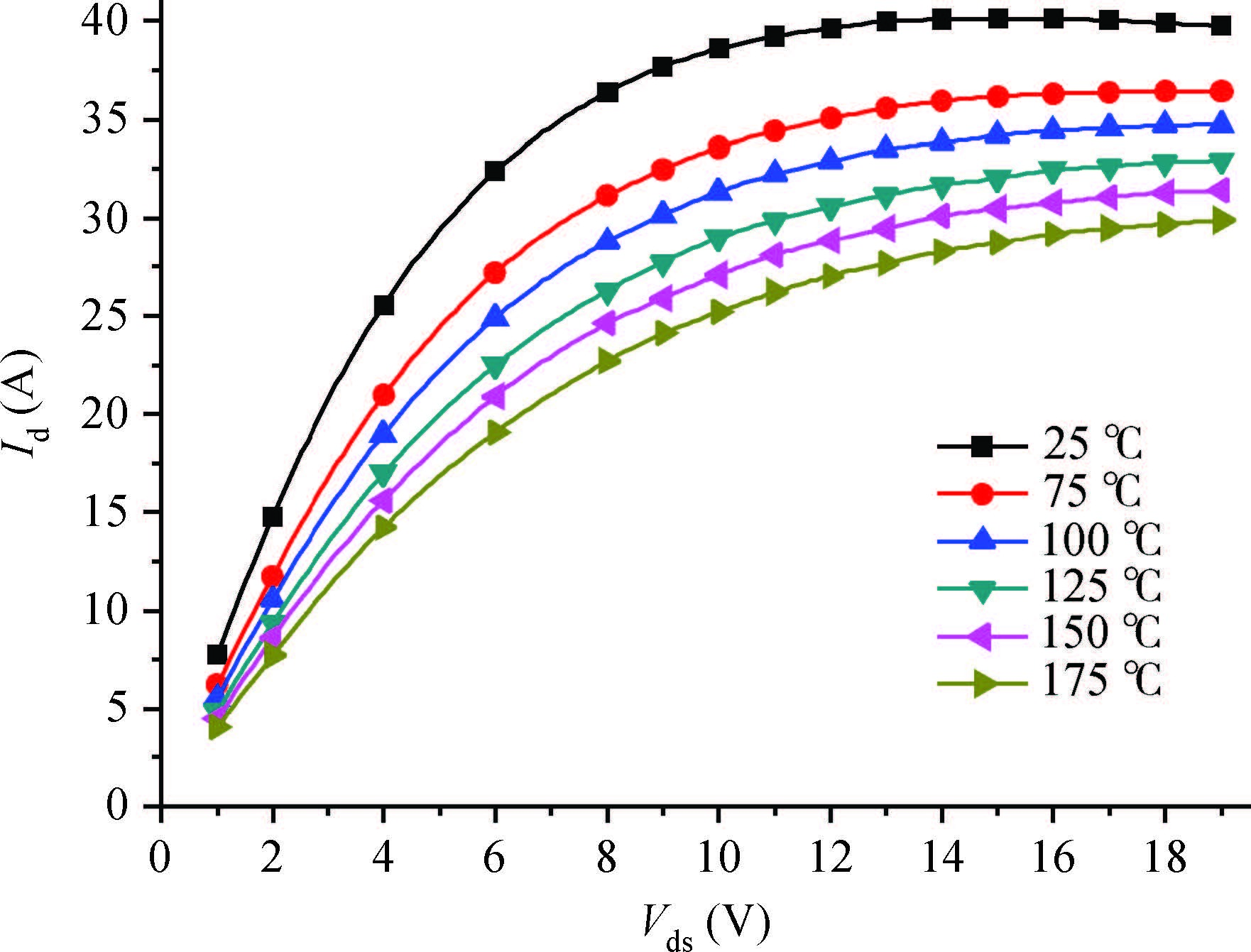
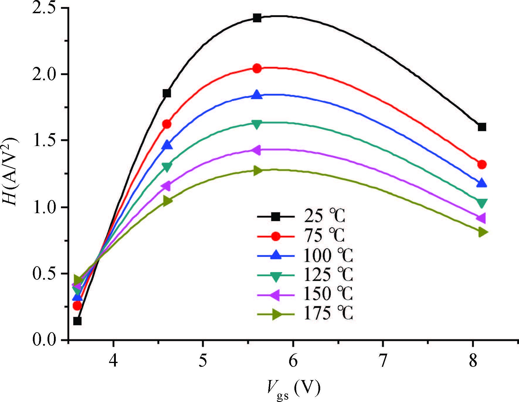
Low-density drain high-electron mobility transistors (LDD-HEMTs) with different F- plasma treatment were investigated by simulations and experiments. The LDD region was performed by introducing negatively charged fluorine ions, which modified the surface field distribution on the drain side of the HEMT, and the enhancement of breakdown voltage were achieved. With the increased fluorine plasma treatment power and LDD region length, the breakdown voltage can be maximumly improved by 70%, and no severe reductions on output current and transconductance were observed. To confirm the temperature stability of the devices, annealing experiments were carried out at 400℃ for 2 min in ambient N2. Moreover, the gate leakage current and breakdown voltage before and after annealing were compared and analyzed, respectively.


J. Semicond.
2016, 37(6): 064010 doi: 10.1088/1674-4926/37/6/064010

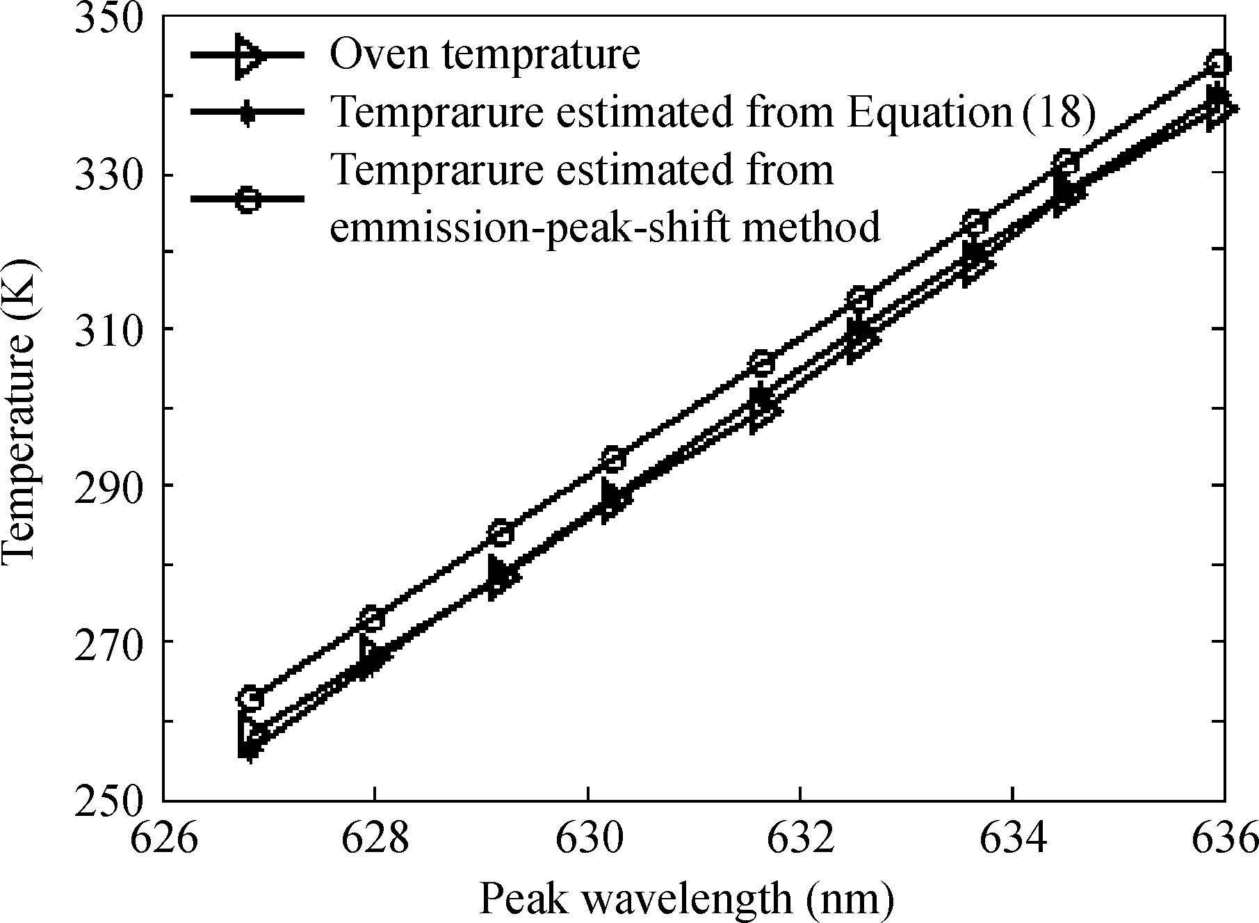
This study proposes a practical method to estimate the junction temperature of AlGaInP LEDs using the luminescence spectra method. The peak wavelength shift of LEDs is due to the energy band gap shrinking. The temperature dependence of the bandgap of AlGaInP LEDs is derived from those of the underlying binary compounds AlP, GaP, and InP. Based on this, a theoretical model for the dependence of the peak wavelength on junction temperature is developed. Experimental results on the junction temperature of AlGaInP red light-emitting diodes are presented. Excellent agreement between the theoretical and experimental temperature dependence of the peak wavelength is found.
J. Semicond.
2016, 37(6): 064011 doi: 10.1088/1674-4926/37/6/064011

The paper investigates the zero temperature coefficient (ZTC) point of power MOSFET, based on the output characteristic of power MOSFET, the temperature coefficient of threshold voltage and the carrier mobility. It is found that the gate voltage has a big effect on the ZTC point. The result indicates that there are three types of temperature coefficient under different gate voltage. When the gate voltage is near the threshold voltage, both the linear region and saturation region shows a large positive temperature coefficient. With the increase of gate voltage, the temperature coefficient of the linear region changes from positive to negative, when the saturation region still remains positive, giving rise to the ZTC point. When the gate voltage is high enough, the negative temperature coefficient is present on both the linear and saturation region, resulting in no ZTC point. According to the experimental result, the change of ZTC point as a function of temperature is larger when the gate voltage is higher. The carrier mobility is also discussed, displaying a positive temperature coefficient at low gate voltage due to the free charge screen effect.

J. Semicond.
2016, 37(6): 064012 doi: 10.1088/1674-4926/37/6/064012
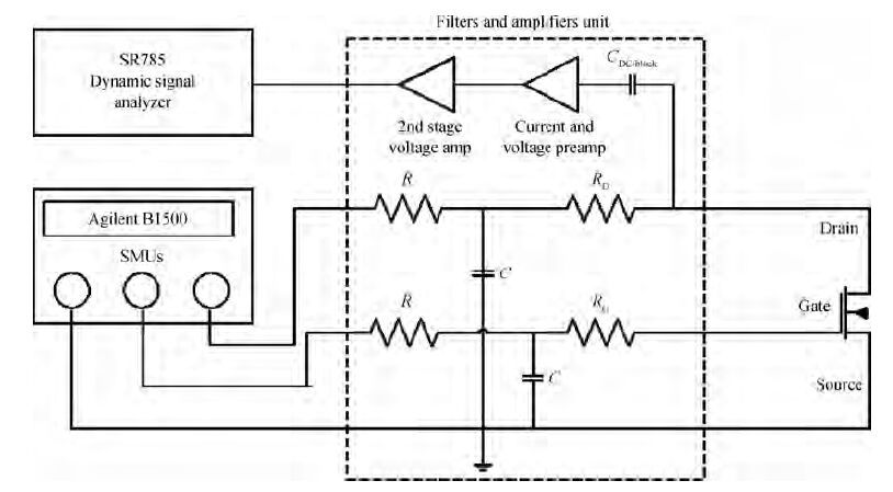
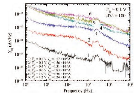
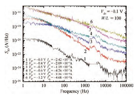
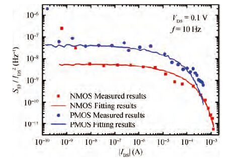
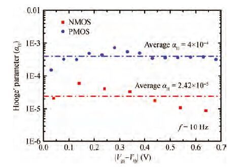
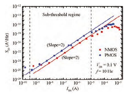
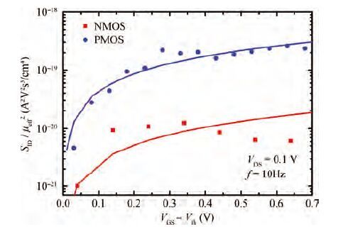
Low-frequency noise behavior in the MOSFETs processed in 65 nm technology is investigated in this paper. Low-frequency noise for NMOS transistors agrees with McWhorter's theory (carrier number fluctuation), low-frequency noise in the sub-threshold regime agrees with McWhorter's theory for PMOS transistors while it agree with Hooge's theory (carrier mobility fluctuation) in the channel strong inversion regime. According to carrier number fluctuation model, the extracted trap densities near the interface between channel and gate oxide for NMOS and PMOS transistor are 3.94×10¹⁷ and 3.56×1018 cm-3/eV respectively. According to carrier mobility fluctuation model, the extracted average Hooge's parameters are 2.42×10⁻⁵ and 4×10⁻⁴. By consideration of BSIM compact model, it is shown that two noise parameters (NOIA and NOIB) can model the intrinsic channel noise. The extracted NOIA and NOIB are constants for PMOS and their values are equal to 3.94×1017 cm-3/eV and 9.31×10⁻⁴ V-1. But for NMOS, NOIA is also a constant while NOIB is inversely proportional to the effective gate voltage. The extracted NOIA and NOIB for NMOS are equal to 3.56×1018 cm-3/eV and 1.53×10⁻² V-1. Good agreement between simulation and experimental results is achieved.

J. Semicond.
2016, 37(6): 064013 doi: 10.1088/1674-4926/37/6/064013

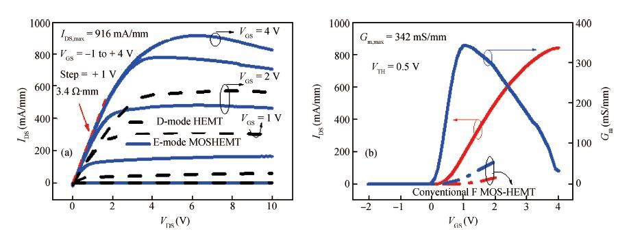
We present high-performance enhancement-mode AlGaN/GaN metal-oxide-semiconductor high-electron mobility transistors (MOS-HEMTs) by a fluorinated gate dielectric technique. A nanolaminate of an Al2O3/LaxAl1-xO3/Al2O3 stack (x≈0.33) grown by atomic layer deposition is employed to avoid fluorine ions implantation into the scaled barrier layer. Fabricated enhancement-mode MOS-HEMTs exhibit an excellent performance as compared to those with the conventional dielectric-last technique, delivering a large maximum drain current of 916 mA/mm and simultaneously a high peak transconductance of 342 mS/mm. The balanced DC characteristics indicate that advanced gate stack dielectrics combined with buffered fluorine ions implantation have a great potential for high speed GaN E/D-mode integrated circuit applications.


J. Semicond.
2016, 37(6): 064014 doi: 10.1088/1674-4926/37/6/064014

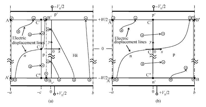
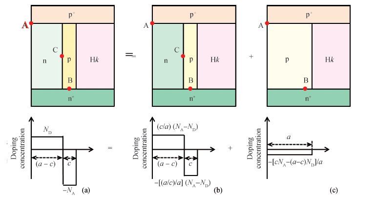
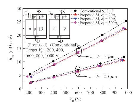
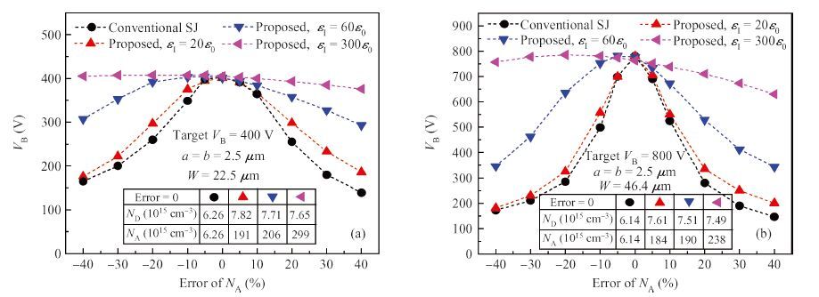
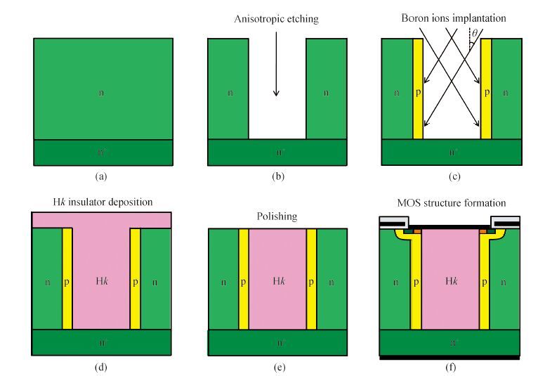
A superjunction (SJ) structure using a high-k (Hk) insulator is studied and optimized by using an analytic model. Results by using the proposed model match well with that of numerical calculations. Numerical calculation results show that, only needing an Hk insulator with a permittivity of εI=5εS, the optimum specific on-resistance of the MOSFET applying the proposed structure is about 8%-20% lower than that of the conventional SJ-MOSFET with VB=200-1000 V. An example with VB=400 V shows that, the permissible error range of doping concentration of the p-region to maintain above 80% of VB is from -37% to +32% for the former and is only from -13% to +13% for the latter.

J. Semicond.
2016, 37(6): 064015 doi: 10.1088/1674-4926/37/6/064015
The internal quantum efficiency (IQE) of the light-emitting diodes can be calculated by the ratio of the external quantum efficiency (EQE) and the light extraction efficiency (LEE). The EQE can be measured experimentally, but the LEE is difficult to calculate due to the complicated LED structures. In this work, a model was established to calculate the LEE by combining the transfer matrix formalism and an in-plane ray tracing method. With the calculated LEE, the IQE was determined and made a good agreement with that obtained by the ABC model and temperature-dependent photoluminescence method. The proposed method makes the determination of the IQE more practical and conventional.


J. Semicond.
2016, 37(6): 064016 doi: 10.1088/1674-4926/37/6/064016
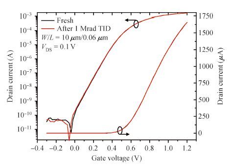
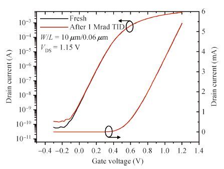
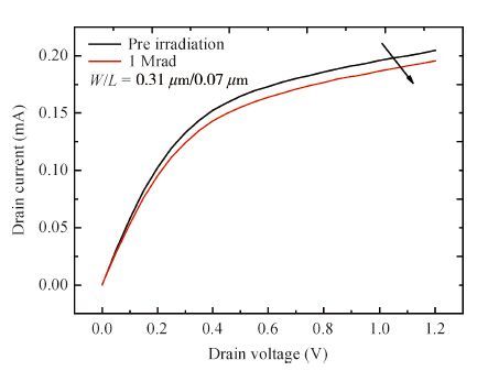
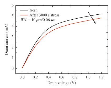
In this paper, total dose responses and reliability issues of MOSFETs fabricated by 65 nm CMOS technology were examined. "Radiation-induced narrow channel effect" is observed in a narrow channel device. Similar to total dose responses of NMOSFETs, narrow channel NMOSFEs have larger hot-carrier-induced degradation than wide channel devices. Step Time-Dependent Dielectric Breakdown (TDDB) stresses are applied, and narrow channel devices have higher breakdown voltage than wide channel devices, which agree with "weakest link" theory of TDDB. Experimental results show that linear current, transconductance, saturated drain current and subthreshold swing are superposed degenerated by total dose irradiation and reliability issues, which may result in different lifetime from that considering total dose irradiation reliability issues separately.


J. Semicond.
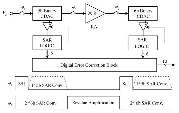
2016, 37(6): 065001 doi: 10.1088/1674-4926/37/6/065001

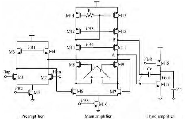
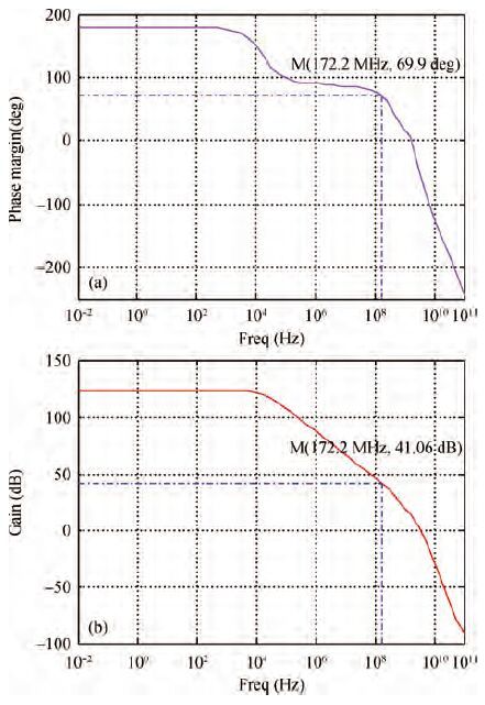
A 10-bit 50 MS/s pipelined SAR ADC is presented which pipelines a 5-bit SAR-based MDAC with a 6-bit SAR ADC. The 1-bit redundancy relaxes the requirement for the sub-ADC decision in accuracy. The SAR-based and "half-gain" MDAC reduce the power consumption and core area. The dynamic comparator and SAR control logic are applied to reduce power consumption. Implemented in 180 nm CMOS, the fabricated ADC achieves 56.04 dB SNDR and 5mW power consumption from 1.8 V power supply at 50 MS/s.


J. Semicond.
2016, 37(6): 065002 doi: 10.1088/1674-4926/37/6/065002
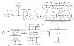
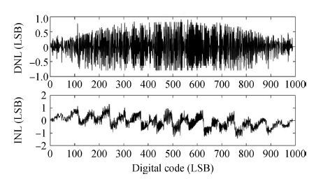
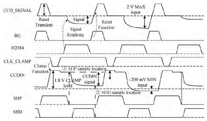
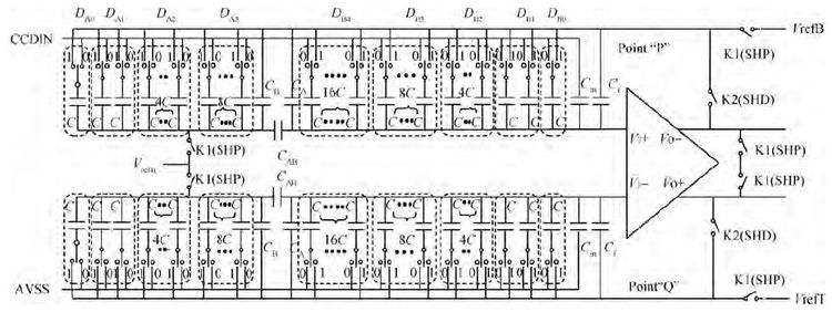
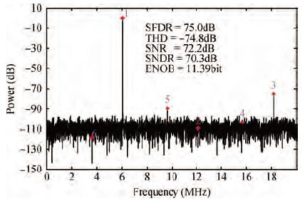
A 14-bit, 40-MHz analog front end (AFE) for CCD scanners is analyzed and designed. The proposed system incorporates a digitally controlled wideband variable gain amplifier (VGA) with nearly 42 dB gain range, a correlated double sampler (CDS) with programmable gain functionality, a 14-bit analog-to-digital converter and a programmable timing core. To achieve the maximum dynamic range, the VGA proposed here can linearly amplify the input signal in a gain range from -1.08 to 41.06 dB in 6.02 dB step with a constant bandwidth. A novel CDS takes image information out of noise, and further amplifies the signal accurately in a gain range from 0 to 18 dB in 0.035 dB step. A 14-bit ADC is adopted to quantify the analog signal with optimization in power and linearity. An internal timing core can provide flexible timing for CCD arrays, CDS and ADC. The proposed AFE was fabricated in SMIC 0.18 μm CMOS process. The whole circuit occupied an active area of 2.8×4.8 mm2 and consumed 360 mW. When the frequency of input signal is 6.069 MHz, and the sampling frequency is 40 MHz, the signal to noise and distortion (SNDR) is 70.3 dB, the effective number of bits is 11.39 bit.


J. Semicond.
2016, 37(6): 065003 doi: 10.1088/1674-4926/37/6/065003
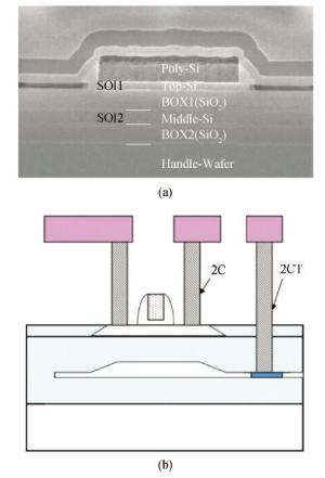
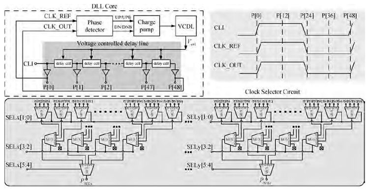
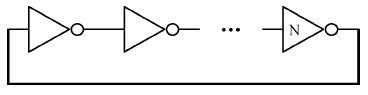
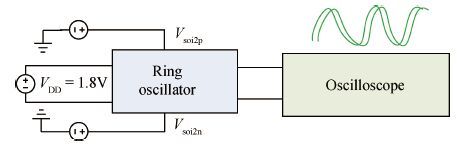
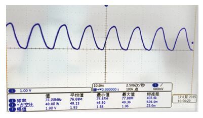
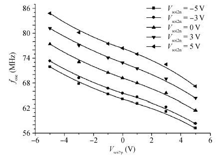
A double silicon on insulator (DSOI) structure was introduced based on fully depleted SOI (FDSOI) technology. The circuit performance could be adjusted dynamically through the separate back gate electrodes applied to N-channel and P-channel devices. Based on DSOI ring oscillator (OSC), this paper focused on the theoretical analysis and electrical test of how the OSC's frequency being influenced by the back gate electrodes (soi2n, soi2p). The testing results showed that the frequency and power consumption of OSC could change nearly linearly along with the back gate bias. According to the different requirements of the circuit designers, the circuit performance could be improved by positive soi2n and negative soi2p, and the power consumption could be reduced by negative soi2n and positive soi2p. The best compromise between performance and power consumption of the circuit could be achieved by appropriate back gate biasing.


J. Semicond.
2016, 37(6): 065004 doi: 10.1088/1674-4926/37/6/065004

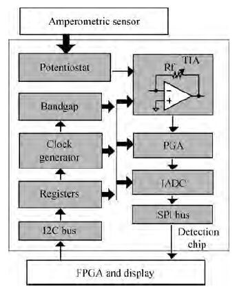
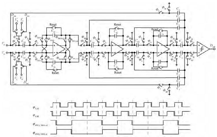
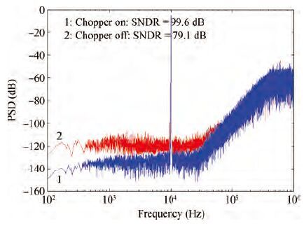
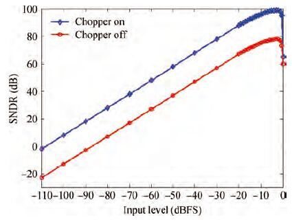
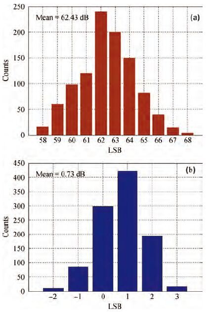
This paper presents a low noise complimentary metal-oxide-semiconductor (CMOS) detection chip for amperometric electrochemical sensors. In order to effectively remove the input offset of the cascaded integrators and the low frequency noise in the modulator, a novel offset cancellation chopping scheme was proposed in the Incremental Δ Σ analog to digital converter (IADC). A novel low power potentiostat was employed in this chip to provide the biasing voltage for the sensor while mirroring the sensor current out for detection. The chip communicates with FPGA through standard built in I2C interface and SPI bus. Fabricated in 0.18-μm CMOS process, this chip detects current signal with high accuracy and high linearity. A prototype microsystem was produced to verify the detection chip performance with current input as well as micro-sensors.


J. Semicond.
2016, 37(6): 065005 doi: 10.1088/1674-4926/37/6/065005
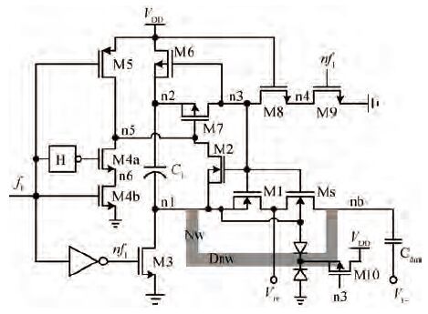
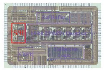
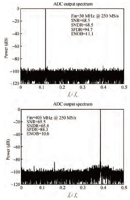
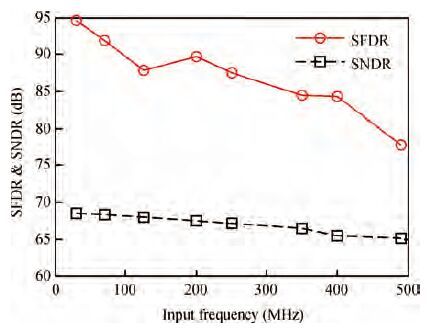
An IF-sampling S/H is presented, which adopts a flip-around structure, bottom-plate sampling technique and improved input bootstrapped switches. To achieve high sampling linearity over a wide input frequency range, the floating well technique is utilized to optimize the input switches. Besides, techniques of transistor load linearization and layout improvement are proposed to further reduce and linearize the parasitic capacitance. The S/H circuit has been fabricated in 0.18-μm CMOS process as the front-end of a 14 bit, 250 MS/s pipeline ADC. For 30 MHz input, the measured SFDR/SNDR of the ADC is 94.7 dB/68. 5dB, which can remain over 84.3 dB/65.4 dB for input frequency up to 400 MHz. The ADC presents excellent dynamic performance at high input frequency, which is mainly attributed to the parasitics optimized S/H circuit.


J. Semicond.
2016, 37(6): 065006 doi: 10.1088/1674-4926/37/6/065006
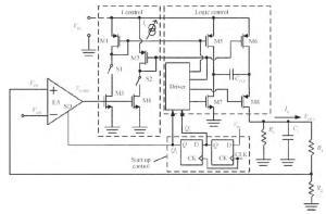
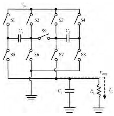
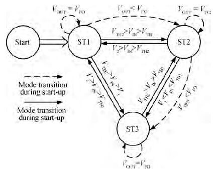
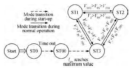
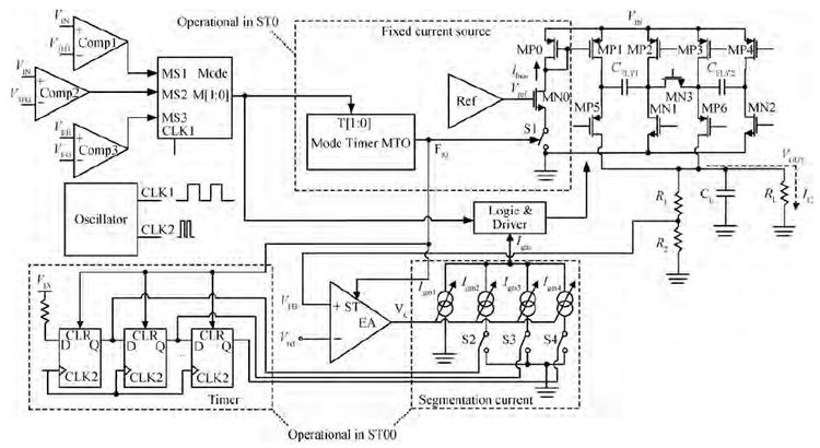
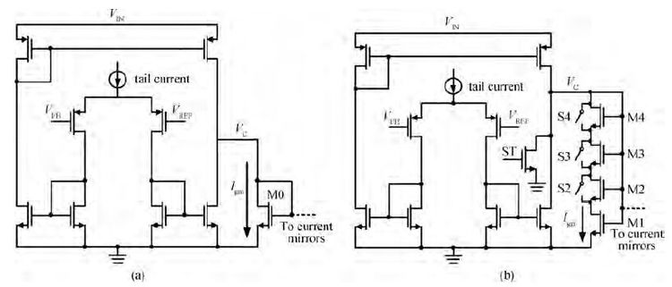
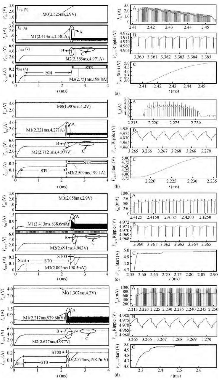
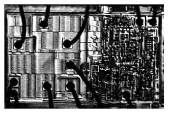
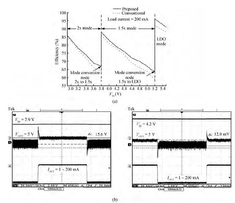
A double-stage start-up structure to limit the inrush current used in current-mode charge pump with wide input range, fixed output and multimode operation is presented in this paper. As a widely utilized power source implement, a Li-battery is always used as the power supply for chips. Due to the internal resistance, a potential drop will be generated at the input terminal of the chip with an input current. A false shut down with a low supply voltage will happen if the input current is too large, leading to the degradation of the Li-battery's service life. To solve this problem, the inrush current is limited by introducing a new start-up state. All of the circuits have been implemented with the NUVOTON 0.6 μm CMOS process. The measurement results show that the inrush current can be limited below 1 A within all input supply ranges, and the power efficiency is higher than the conventional structure.


J. Semicond.
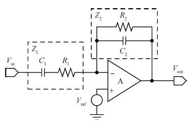
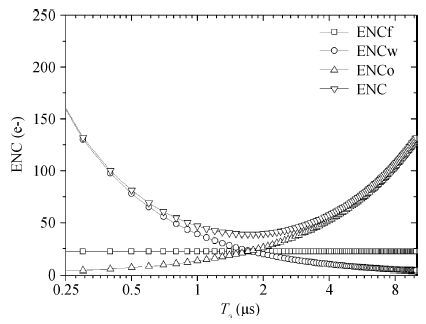
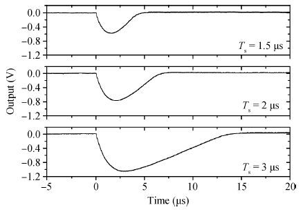
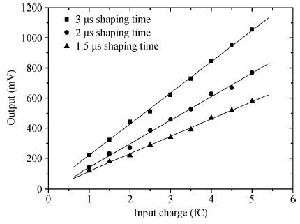
2016, 37(6): 065007 doi: 10.1088/1674-4926/37/6/065007
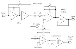
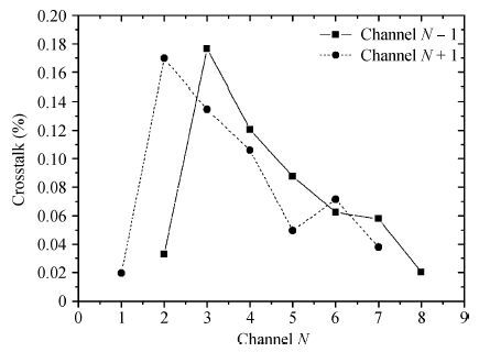
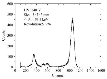
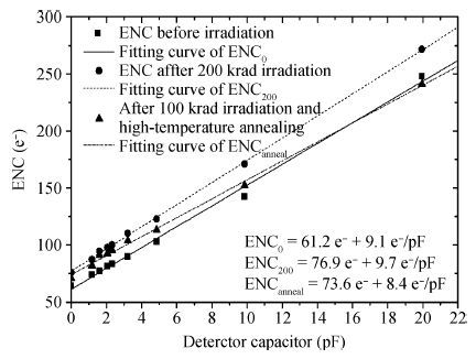
In this paper, we present the design and performances of a low-noise and radiation-hardened front-end readout application specific integrated circuit (ASIC) dedicated to CdZnTe detectors for a hard X-ray imager in space applications. The readout channel is comprised of a charge sensitive amplifier, a CR-RC shaping amplifier, an analog output buffer, a fast shaper, and a discriminator. An 8-channel prototype ASIC is designed and fabricated in TSMC 0.35-μm mixed-signal CMOS technology, the die size of the prototype chip is 2.2×2.2 mm2. The input energy range is from 5 to 350 keV. For this 8-channel prototype ASIC, the measured electrical characteristics are as follows:the overall gain of the readout channel is 210 V/pC, the linearity error is less than 2%, the crosstalk is less than 0.36%, The equivalent noise charge of a typical channel is 52.9 e- at zero farad plus 8.2 e- per picofarad, and the power consumption is less than 2.4 mW/channel. Through the measurement together with a CdZnTe detector, the energy resolution is 5.9% at the 59.5-keV line under the irradiation of the radioactive source 241Am. The radiation effect experiments show that the proposed ASIC can resist the total ionization dose (TID) irradiation of higher than 200 krad(Si).