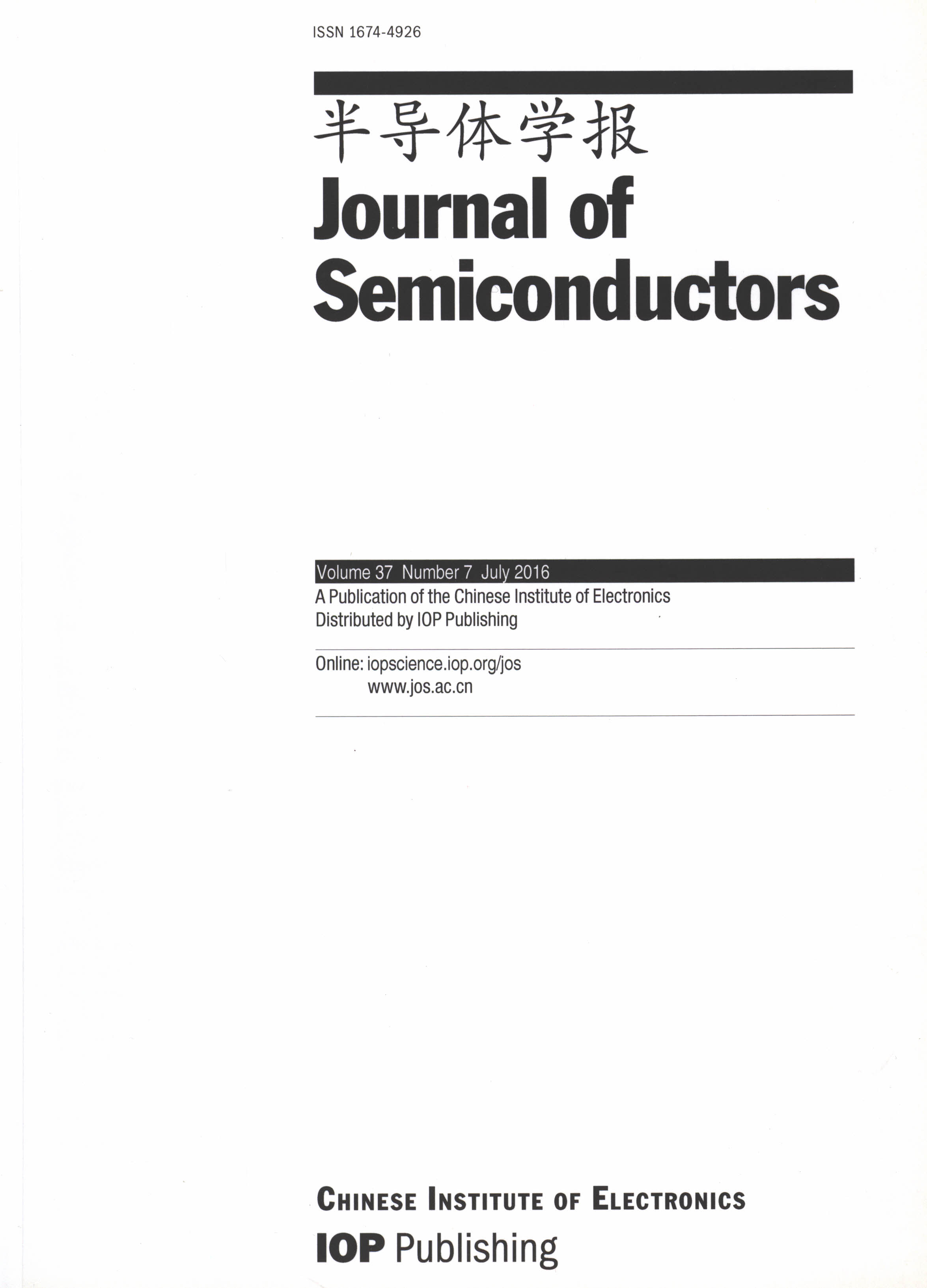
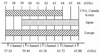
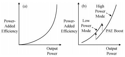
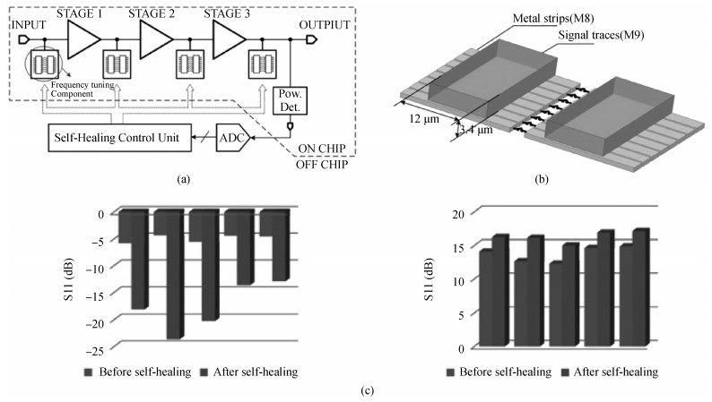
The challenges in the design of CMOS millimeter-wave (mm-wave) transceiver for Gbps wireless communication are discussed. To support the Gbps data rate, the link bandwidth of the receiver/transmitter must be wide enough, which puts a lot of pressure on the mm-wave front-end as well as on the baseband circuit. This paper discusses the effects of the limited link bandwidth on the transceiver system performance and overviews the bandwidth expansion techniques for mm-wave amplifiers and IF programmable gain amplifier. Furthermore, dual-mode power amplifier (PA) and self-healing technique are introduced to improve the PA's average efficiency and to deal with the process, voltage, and temperature variation issue, respectively. Several fully-integrated CMOS mm-wave transceivers are also presented to give a short overview on the state-of-the-art mm-wave transceivers.


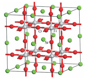
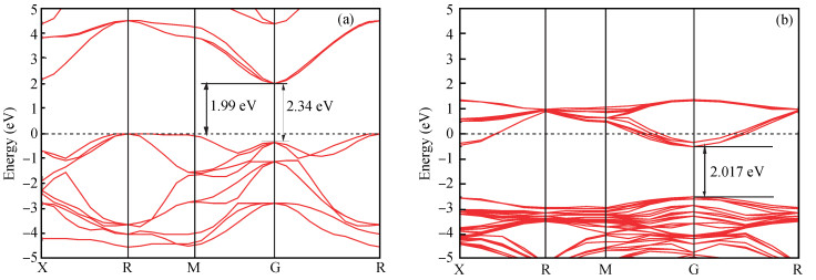
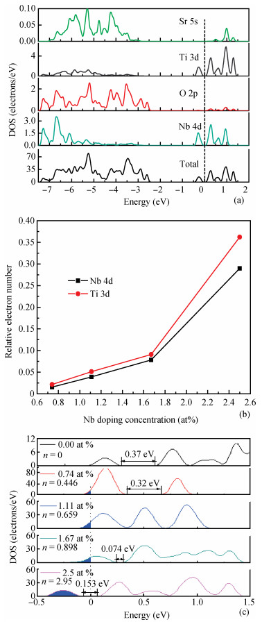
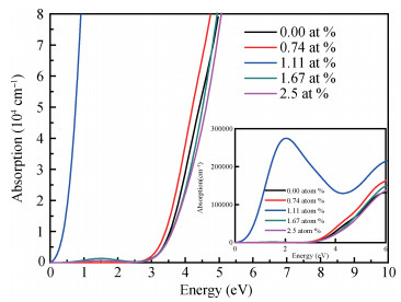
The n-type Nb-doped SrTiO3 with different doping concentrations were studied by first principles calculations. The effects of Nb concentration on the formation enthalpy, electronic structure and optical property were investigated. Results show that Nb preferentially enters the Ti site in SrTiO3, which is in good agreement with the experimental observation. The Fermi level of Nb-doped SrTiO3 moves into the bottom of the conduction band, and the system becomes an n-type semiconductor. The effect of Nb-doping concentration on the conductivity was discussed from the microscopic point of view. Furthermore, the 1.11 at% Nb-doped SrTiO3 shows strong absorption in the visible light and becomes a very useful material for photo-catalytic activity. The 1.67 at% and 2.5 at% Nb-doped models will be potential transparent conductive materials.

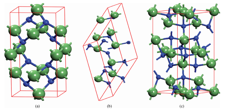
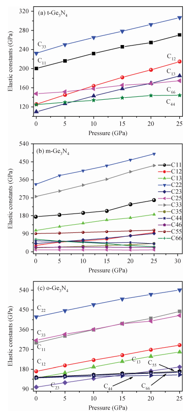
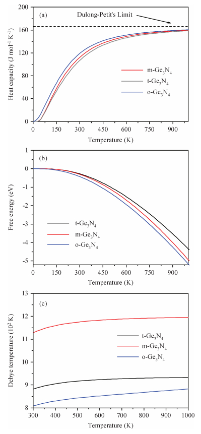
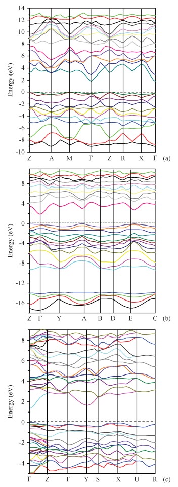
The ultrasoft pseudo-potential plane wave method combined with the quasi-harmonic approach have been used to study the electronic, elastic and thermodynamic properties of the tetragonal, monoclinic and orthorhombic Ge3N4. The negative formation enthalpies, the satisfactory of Born's criteria and the linear variations of elastic constants with pressure indicate that the three polymorphs can retain their stabilities in the pressure range of 0-25 GPa. The three Ge3N4 are brittle solids at 0 GPa, while they behave in ductile manners in the pressure range of 5-25 GPa. t- and o-Ge3N4 are hard materials but anisotropic. m-Ge3N4 has the largest ductility among the three phases. The results reveal that m-Ge3N4 belongs to an indirect band gap semiconductor, while t- and o-Ge3N4 have direct band gaps. For the thermal properties, several interesting features can be observed above 300 K. o-Ge3N4 exhibits the largest heat capacity, while m-Ge3N4 shows the highest Debye temperature. The results predicted in this work can provide reference data for future experiments.

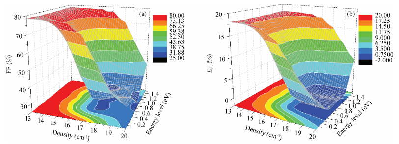
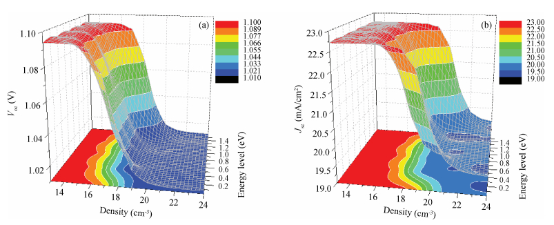
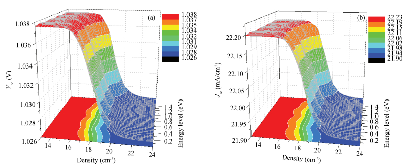
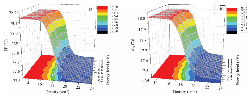
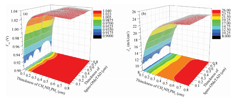
We built an ideal perovskite solar cell model and investigated the effects of defect states on the solar cell's performance. The verities of defect states with a different energy level in the band gap and those in the absorption layer CH3NH3PbI3 (MAPbI3), the interface between the buffer layer/MAPbI3, and the interface between the hole transport material (HTM) and MAPbI3, were studied. We have quantitatively analyzed these effects on perovskite solar cells' performance parameters. They are open-circuit voltage, short-circuit current, fill factor, and photoelectric conversion efficiency. We found that the performances of perovskite solar cells change worse with defect state density increasing, but when defect state density is lower than 1016 cm-3, the effects are small. Defect states in the absorption layer have much larger effects than those in the adjacent interface layers. The perovskite solar cells have better performance as its working temperature is reduced. When the thickness of MAPbI3 is about 0.3 μm, perovskite solar cells show better comprehensive performance, while the thickness 0.05 μm for Spiro-OMeTAD is enough.


CuPt-type ordering with undesirable properties always occurs in GaInP at growth conditions that are very close to those leading to the highest quality material in metal organic chemical vapor deposition. In this work, highly disordered GaInP with high crystalline quality was obtained by optimizing growth conditions. Room-temperature and low-temperature photoluminescence (PL) spectra of AlGaInP/GaInP/AlGaInP double heterostructures (DHs) reveal that the band edge emission intensity is enhanced by optimizing growth temperature, V/Ⅲ ratio, and reactor pressure at the expense of low energy peak originating from spatially indirect recombination due to the ordering-related defects. The DH sample with less ordering-related defects demonstrates a longer effective minority carrier lifetime, consequently, the GaInP solar cell shows a significant improvement in the performance.


The carbon nanotube field effect transistor (CNTFET) is modelled for circuit application. The model is based on the transport mechanism and it directly relates the transport mechanism with the chirality. Also, it does not consider self consistent equations and thus is used to develop the HSPICE compatible circuit model. For validation of the model, it is applied to the top gate CNTFET structure and the MATLAB simulation results are compared with the simulations of a similar structure created in NanoTCAD ViDES. For demonstrating the circuit compatibility of the model, two circuits viz. inverter and SRAM are designed and simulated in HSPICE. Finally, SRAM performance metrics are compared with those of device simulations from NanoTCAD ViDES.


The present paper discusses the performance of ITO/PEDOT:PSS/n-SnS/Al structured solar cells fabricated by thermal evaporation. The performance characterizing parameters such as the open circuit voltage, short circuit current density, series resistance, parallel resistance, ideality factor and the overall efficiency were found to be dependent on the SnS grain size in the nano-meter regime and incident light intensity. The experimental work directly reconfirms the theoretical results and ideas raised in the literature by early researchers.


The 100-nm T-gate InP-based InAlAs/InGaAs high electron mobility transistors (HEMTs) with the width of 2×50 μm and source-drain space of 2.4 μm are systematically investigated. High indium (In) composition of InGaAs layer was adopted to acquire the higher mobility of the channel layer. A sandwich structure was adopted to optimize the cap layers and produce a very low contact resistance. The fabricated devices exhibit extrinsic maximum transconductance Gm.max=1441 mS/mm, cutoff frequency fT=260 GHz, and maximum oscillation frequency fmax=607 GHz. A semi-empirical model has been developed to precisely fit the low-frequency region of scattering parameters (S parameters) for InP-based HEMTs. Excellent agreement between measured and simulated S parameters demonstrates the validity of this approach.


A new semi-insulation structure in which one isolated island is connected to the substrate was proposed. Based on this semi-insulation structure, an advanced BCD technology which can integrate a vertical device without extra internal interconnection structure was presented. The manufacturing of the new semi-insulation structure employed multi-epitaxy and selectively multi-doping. Isolated islands are insulated with the substrate by reverse-biased PN junctions. Adjacent isolated islands are insulated by isolation wall or deep dielectric trenches. The proposed semi-insulation structure and devices fixed in it were simulated through two-dimensional numerical computer simulators. Based on the new BCD technology, a smart power integrated circuit was designed and fabricated. The simulated and tested results of Vertical DMOS, MOSFETs, BJTs, resistors and diodes indicated that the proposed semi-insulation structure is reasonable and the advanced BCD technology is validated.


The insulated gate bipolar transistor (IGBT) has negative Miller capacitance during switching transients. It has conventionally been attributed to the voltage dependency of the Miller capacitance. However this explanation has physical ambiguity, yet, it lacks a discussion of the conditions for the occurrence of negative Miller capacitance as well. We argue that it is the current dependence to the Miller capacitance that results in the negative case. In this paper, we provide a modification to the theoretical analysis of this phenomenon. The occurrence condition for it and the device parameters about it are discussed. It is discovered that the negative Miller capacitance must occur during the turn-off process for any IGBT, while it is relatively difficult during the turn-on process. At the device design level, the current gain of the PNP transistor in the IGBT is an important factor for the negative Miller capacitance.


Accurate modeling of the electrothermal effects of GaN electronic devices is critical for reliability design and assessment. In this paper, an improved temperature-dependent model for large signal equivalent circuit modeling of GaN HEMTs is proposed. To accurately describe the thermal effects, a modified nonlinear thermal sub-circuit which is related not only to power dissipation, but also ambient temperature is used to calculate the variations of channel temperature of the device; the temperature-dependent parasitic and intrinsic elements are also taken into account in this model. The parameters of the thermal sub-circuit are extracted by using the numerical finite element method. The results show that better performance can be achieved by using the proposed large signal model in the range of -55 to 125℃ compared with the conventional model with a linear thermal sub-circuit.


The bottom-gate structure ZnO based thin film transistors (ZnO-TFTs) using Bi1.5Zn1.0Nb1.5O7 (BZN) thin films as gate insulator were fabricated on Pt/SiO2/Si substrate by radio frequency magnetic sputtering. We investigated the effect of annealing temperature at 300, 400, and 500℃ on the performance of BZN thin films and ZnO-TFTs. XRD measurement confirmed that BZN thin films were amorphous in nature. BZN thin films annealed at 400℃ obtain the high capacitance density of 249 nF/cm2, high dielectric constant of 71, and low leakage current density of 10-7 A/cm2 on/off current ratio and field effect mobility of ZnO-TFTs annealed at 400℃ are approximately one order of magnitude and two times, respectively higher than that of ZnO-TFTs annealed at 300℃. When the annealing temperature is 400℃, the electrical performance of ZnO-TFTs is enhanced remarkably. Devices obtain a low sub-threshold swing of 470 mV/dec and surface states density of 3.21×1012cm-2.


This paper describes and analyses the impact of the Ti layer, which is embedded between the insulator and top electrode, on the programming characteristic of the Al-HfO2-Al antifuse. The programming voltage of the antifuse with 120 Å HfO2 is properly reduced from 5.5 to 4.6 V with an embedded Ti layer. Low on-state resistance (~19 Ω) and low programming voltage (4.6 V) is demonstrated in the embedded Ti antifuse with 120 Å HfO2 while keeping sufficient off-state reliability. The antifuse embedded with a Ti layer between the insulator and top electrode has been developed and has potential in field programmable devices.


In this paper, we present the simulation and fabrication of a thin film bulk acoustic resonator (FBAR). In order to improve the accuracy of simulation, an improved Mason model was introduced to design the resonator by taking the coupling effect between electrode and substrate into consideration. The resonators were fabricated by the eight inch CMOS process, and the measurements show that the improved Mason model is more accurate than a simple Mason model. The Qs (Q at series resonance), Qp (Q at parallel resonance), Qmax and kt2 of the FBAR were measured to be 695, 814, 1049, and 7.01% respectively, showing better performance than previous reports.


In order to verify which of the distributions and established methods of reliability model are more suitable for the analysis of the accelerated aging of LED lamp, three established methods (approximate method, analytical method and two-stage method) of reliability model are used to analyze the experimental data under the condition of the Weibull distribution and Lognormal distribution, in this paper. Ten LED lamps are selected for the accelerated aging experiment and the luminous fluxes are measured at an accelerated aging temperature. AIC information criterion is adopted in the evaluation of the models. The results show that the accuracies of the analytical method and the two-stage method are higher than that of the approximation method, with the widths of confidence intervals of unknown parameters of the reliability model being the smallest for the two-stage method. In a comparison between the two types of distributions, the accuracies are nearly identical.


For 3D vertical NAND flash memory, the charge pump output load is much larger than that of the planar NAND, resulting in the performance degradation of the conventional Dickson charge pump. Therefore, a novel all PMOS charge pump with high voltage boosting efficiency, large driving capability and high power efficiency for 3D V-NAND has been proposed. In this circuit, the Pelliconi structure is used to enhance the driving capability, two auxiliary substrate bias PMOS transistors are added to mitigate the body effect, and the degradation of the output voltage and boost efficiency caused by the threshold voltage drop is eliminated by dynamic gate control structure. Simulated results show that the proposed charge pump circuit can achieve the maximum boost efficiency of 86% and power efficiency of 50%. The output voltage of the proposed 9 stages charge pump can exceed 2 V under 2 MHz clock frequency in 2X nm 3D V-NAND technology. Our results provide guidance for the peripheral circuit design of high density 3D V-NAND integration.


The bufferless router emerges as an interesting option for cost-efficient in network-on-chip (NoC) design. However, the bufferless router only works well under low network load because deflection more easily occurs as the injection rate increases. In this paper, we propose a load balancing bufferless deflection router (LBBDR) for NoC that relieves the effect of deflection in bufferless NoC. The proposed LBBDR employs a balance toggle identifier in the source router to control the initial routing direction of X or Y for a flit in the network. Based on this mechanism, the flit is routed according to XY or YX routing in the network afterward. When two or more flits contend the same one desired output port a priority policy called nearer-first is used to address output ports allocation contention. Simulation results show that the proposed LBBDR yields an improvement of routing performance over the reported bufferless routing in the flit deflection rate, average packet latency and throughput by up to 13%, 10% and 6% respectively. The layout area and power consumption compared with the reported schemes are 12% and 7% less respectively.


An ultra-high-frequency (UHF) radio frequency identification (RFID) secure tag chip with a non-crypto mode and a crypto mode is presented. During the supply chain management, the tag works in the non-crypto mode in which the on-chip crypto engine is not enabled and the tag chip has a sensitivity of -12.8 dBm for long range communication. At the point of sales (POS), the tag will be switched to the crypto mode in order to protect the privacy of customers. In the crypto mode, an advanced encryption standard (AES) crypto engine is enabled and the sensitivity of the tag chip is switched to +2 dBm for short range communication, which is a method of physical protection. The tag chip is implemented and verified in a standard 0.13-μm CMOS process.


Several improvements have been made to the conventional segmented linear light-emitting diode (LED) driver topology to enhance the performance and reliability of the system. A compensation technology is proposed to adaptively adjust the impedance of the sensing circuit to keep the output luminance constant in case of line voltage variations. Based on the proposed technology, an active over temperature protection technique is presented to constrain the averaged LED current according to the junction temperature to prevent the driving IC from overheating. Otherwise, a pulse width modulation dimming circuitry which is compatible with input logic level ranging from 1.8 to 20 V is proposed. The proposed technologies are implemented in a 1.0 μm 5/20/500 V BCD technology with three high voltage MOSFETs integrated on chip. The experimental results show that within 220±15% V, 50 Hz AC line-voltage variation, the output luminance is restrained to 4% in total. The output luminance can also be effectively controlled by the PWM dimming circuitry, and a dimming range of 95% is achieved with good linearity.


This paper presents a 10-bit 50-MS/s subrange successive-approximation register (SAR) analog-to-digital converter (ADC) composed of a 4-bit SAR coarse ADC and a 6-bit SAR fine ADC. In the coarse ADC, multi-comparator SAR architecture is used to reduce the digital logic propagation delay, and a traditional asynchronous SAR ADC with monotonic switching method is used as the fine ADC. With that combination, power dissipation also can be much reduced. Meanwhile, a modified SAR control logic is adopted in the fine ADC to speed up the conversion and other techniques, such as splitting capacitors array, are borrowed to reduce the power consumption. Fabricated with 1P8M 130-nm CMOS technology, the proposed SAR ADC achieves 51.6-dB signal to noise and distortion ratio (SNDR) and consumes 186 μ W at 50 MS/s with a 1-V supply, resulting in a figure of merit (FOM) of 12 fJ/conversion-step. The core area is only 0.045 mm2.