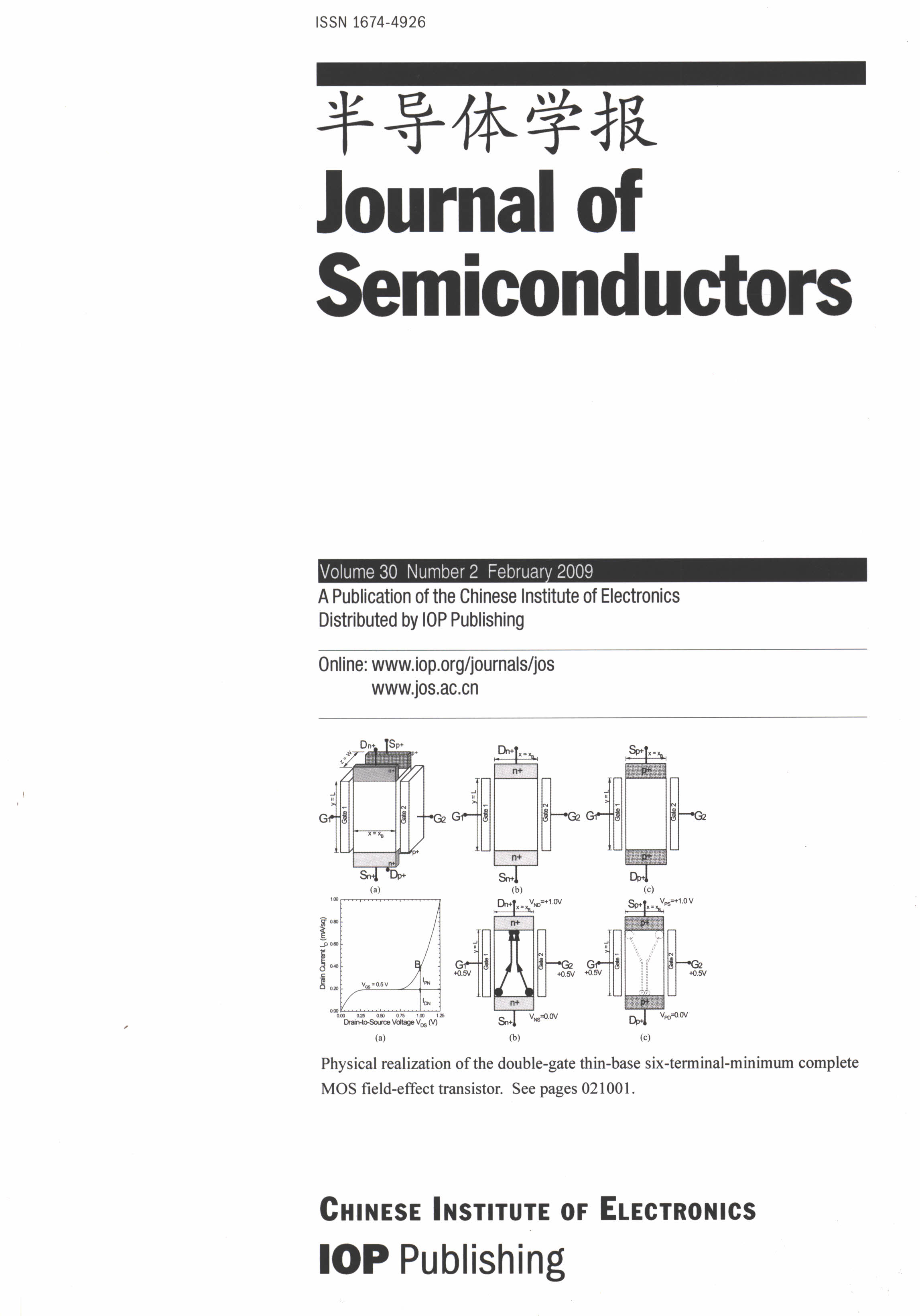
This paper reports the physical realization of the Bipolar Field-Effect Transistor (BiFET) and its one-transistor basic building block circuits. Examples are given for the one and two MOS gates on thin and thick, pure and impure base, with electron and hole contacts, and the corresponding theoretical current–voltage characteristics previously computed by us, without generation-recombination-trapping-tunneling of electrons and holes. These examples include the one-MOS-gate on semi-infinite thick impure base transistor (the bulk transistor) and the impure-thin-base Silicon-on-Insulator (SOI) transistor and the two-MOS-gates on thin base transistors (the FinFET and the Thin Film Transistor TFT). Figures are given with the cross-section views containing the electron and hole concentration and current density distributions and trajectories and the corresponding DC current–voltage characteristics.
A semiconductor PEC etching method is applied to fabricate the n-type silicon deep micropore channel array. In this method, it is important to arrange the direction of the micropore array along the crystal orientation of the Si substrate. Otherwise, serious lateral erosion will happen. The etching process is also relative to the light intensity and HF concentration. 5% HF concentration and 10–15 cm distance between the light source and the silicon wafer are demonstrated to be the best in our experiments. The n-type silicon deep micropore channel array with aperture of 3 mm and aspect ratio of 40–60, whose inner walls are smooth, is finally obtained.
Transparent conducting zirconium-doped zinc oxide films with high transparency and relatively low resistivity have been successfully prepared on water-cooled glass substrate by radio frequency magnetron sputtering at room temperature. The Ar sputtering pressure was varied from 0.5 to 3 Pa. The crystallinity increases and the electrical resistivity decreases when the sputtering pressure increases from 0.5 to 2.5 Pa. The cystallinity decreases and the electrical resistivity increases when the sputtering pressure increases from 2.5 to 3 Pa. When the sputtering pressure is 2.5 Pa, it is obtained that the lowest resistivity is 2.03 × 10⁻⁵ Ω·cm with a very high transmittance of above 94%. The deposited films are polycrystalline with a hexagonal structure and a preferred orientation perpendicular to the substrate.
We investigate the thermal stability of HfTaON films prepared by physical vapor deposition using high resolution transmission electronic microscope (HRTEM) and X-ray photoelectron spectroscopy (XPS). The results indicate that the magnetron-sputtered HfTaON films on Si substrate are not stable during the post-deposition annealing (PDA). HfTaON will react with Si and form the interfacial layer at the interface between HfTaON and Si substrate. Hf–N bonds are not stale at high temperature and easily replaced by oxygen, resulting in significant loss of nitrogen from the bulk film. SiO buffer layer introduction at the interface of HfTaON and Si substrate may effectively suppress their reaction and control the formation of thicker interfacial layer. But SiO is a low k gate dielectric and too thicker SiO buffer layer will increase the gate dielectric's equivalent oxide thickness. SiON prepared by oxidation of N-implanted Si substrate has thinner physical thickness than SiO and is helpful to reduce the gate dielectric's equivalent oxide thickness.
Chemical mechanical polishing (CMP) has been used to produce smooth and scratch-free surfaces for GaN. In the aqueous solution of KOH, GaN is subjected to etching. At the same time, all surface irregularities, including etch pyramids, roughness after mechanical polishing and so on will be removed by a polishing pad. The experiments had been performed under the condition of different abrasive particle sizes of the polishing pad. Also the polishing results for different polishing times are analyzed, and chemical mechanical polishing resulted in an average root mean square (RMS) surface roughness of 0.565 nm, as measured by atomic force microscopy.
A surface potential based non-charge-sheet core model for cylindrical undoped surrounding-gate (SRG) MOSFETs is presented. It is based on the exact surface potential solution of Poisson's equation and Pao-Sah's dual integral without the charge-sheet approximation, allowing the SRG-MOSFET characteristics to be adequately described by a single set of the analytic drain current equation in terms of the surface potential evaluated at the source and drain ends. It is valid for all operation regions and traces the transition from the linear to saturation and from the sub-threshold to strong inversion region without fitting-parameters, and verified by the 3-D numerical simulation.
The performance of a partially depleted silicon-on-insulator (PDSOI) dynamic threshold MOSFET (DTMOS) is degraded by the large body capacitance and body resistance. Increasing silicon film thickness can reduce the body resistance greatly, but the body capacitance also increases significantly at the same time. To solve this problem, a novel SOI DTMOSFET structure (drain/source-on-local-insulator structure) is proposed. From ISE simulation, the improvement in delay, obtained by optimizing p-n junction depth and silicon film thickness, is very significant. At the same time, we find that the drive current increases significantly as the thickness of the silicon film increases. Furthermore, only one additional mask is needed to form the local SIMOX, and other fabrication processes are fully compatible with conventional CMOS/SOI technology.
A complex-coupled DFB laser with sampled grating has been designed and fabricated. The method uses the +1st order reflection of the sampled grating for laser single-mode operation. The typical threshold current of the sampled grating based DFB laser is 25 mA, and the optical output is about 10 mW at the injected current of 100 mA. The lasing wavelength of the device is 1.5385 µm, which is the +1st order wavelength of the sampled grating.
Novel physical models for leakage current analysis in 65 nm technology are proposed. Taking into consideration the process variations and emerging effects in nano-scaled technology, the presented models are capable of accurately estimating the subthreshold leakage current and junction tunneling leakage current in 65??nm technology. Based on the physical models, new table look-up models are developed and first applied to leakage current analysis in pursuit of higher simulation speed. Simulation results show that the novel physical models are in excellent agreement with the data measured from the foundry in the 65 nm process, and the proposed table look-up models can provide great computational efficiency by using suitable interpolation techniques. Compared with the traditional physical-based models, the table look-up models can achieve 2.5X speedup on average on a variety of industry circuits.
Based on the difference close-loop feedback technique and the difference pre-amp, a high efficiency PWM CMOS class-D audio power amplifier is proposed. A rail-to-rail PWM comparator with window function has been embedded in the class-D audio power amplifier. Design results based on the CSMC 0.5 mm CMOS process show that the max efficiency is 90%, the PSRR is –75 dB, the power supply voltage range is 2.5–5.5 V, the THD+N in 1 kHz input frequency is less than 0.20%, the quiescent current in no load is 2.8 mA, and the shutdown current is 0.5 mA. The active area of the class-D audio power amplifier is about 1.47 × 1.52 mm2. With the good performance, the class-D audio power amplifier can be applied to several audio power systems.
A 4–9 GHz wideband high power amplifier is designed and fabricated, which has demonstrated saturated output power of 10 W covering 6–8 GHz band, and above 6 W over the other band. This PA module uses a balance configuration, and presents power gain of 7.3 ± 0.9 dB over the whole 4–9 GHz band and 39% power-added efficiency (PAE) at 8 GHz. Both the input and output VSWR are also excellent, which are bellow –10 dB.
A low power linear stepping digital programming gain amplifier (PGA) is designed for CMOS image sensors. The PGA consists of three stages with gain range from one to nine. The gain is divided into four regions and each range has 128 linear steps. Power consumption of the PGA is saved by good tradeoff between variation of amplifier feedback coefficient, pipeline stages and gain regions. With thermometer-binary mixed coding and linear pipeline gain stepping, the load capacitance keeps constant when the gain of one stage is changed. The PGA is designed in the SMIC 0.18 µm process. Simulation results show that the power consumption is 3.2 mW with 10 bit resolution and 10 MSPS sampling rate. The PGA has been embedded in a 0.3 megapixel CMOS image sensors and fabricated successfully.
A CMOS quadrature LC-tank voltage-controlled oscillator topology which uses a planar spiral transformer as coupling elements has been implemented in mixed-signal and RF 1P6M 0.18 mm CMOS technology of SMIC. The measured phase noise is –125.7 dBc/Hz at an offset frequency of 1 MHz from the carrier of 4.6 GHz while the VCO core circuit draws only of 10 mW from a 1.8 V supply. The measured phase error is approximately 1.5 based on the time domain outputs and the output power is about –2 dBm. The VCO can cover the frequency range of 4.36–4.68 GHz. The tuning range is 320 MHz (7.0%) and the FOM is –189 dB.
A 6 GHz voltage controlled oscillator (VCO) optimized for power and noise performance was designed and characterized. This VCO was designed with the negative-resistance (Neg-R) method, utilizing an InGaP/GaAs hetero-junction bipolar transistor in the negative-resistance block. A proper output matching network and a high Q stripe line resonator were used to enhance output power and depress phase noise. Measured central frequency of the VCO was 6.008 GHz. The tuning range was more than 200 MHz. At the central frequency, an output power of 9.8 dBm and phase noise of –122.33 dBc/Hz at 1 MHz offset were achieved, the calculated RF to DC efficiency was about 14%, and the figure of merit was –179.2 dBc/Hz.
A 13-bit 8 MSample/s high-accuracy CMOS pipeline ADC is proposed. At the input, the sample-and-hold amplifier (SHA) is removed for low power and low noise; meanwhile, an improved sampling circuit is adopted to alleviate the clock skew effect. On-chip bias current is programmable to achieve low power dissipation at different sampling rates. Particularly, drain-to-source voltages in the operational amplifiers (opamps) are fixed to ensure high DC gain within the variant range of the bias current. Both on-chip and off-chip decoupling capacitors are used in the voltage reference circuit in consideration of low power and stability. The proposed ADC was implemented in 0.18-mm 1P6M CMOS technology. With a 2.4-MHz input, the measured peak SNDR and SFDR are 74.4 and 91.6 dB at 2.5 MSample/s, 74.3 and 85.4 dB at 8.0 MSample/s. It consumes 8.1, 21.6, 29.7, and 56.7 mW (including I/O drivers) when operating at 1.5, 2.5, 5.0, and 8.0 MSample/s with 2.7 V power supply, respectively. The chip occupies 3.2 mm, including I/O pads.
A current-mode buck DC–DC controller based on adaptive on-time (AOT) control is presented. The on-time is obtained by the techniques of input feedforward and output feedback, and the adaptive control is achieved by a sample-hold and time-ahead circuit. The AOT current-mode control scheme not only obtains excellent transient response speed, but also achieves the independence of loop stability on output capacitor ESR. In addition, the AOT current-mode control does not have subharmonic oscillation phenomenon seen in fixed frequency peak current-mode control, so there is no need of the slope compensation circuit. The auto-skip pulse frequency modulation (PFM) mode improves the conversion efficiency of light load effectively. The controller has been fabricated with UMC 0.6-µm BCD process successfully and the detailed experimental results are shown.
This work presents an ultra-high speed 2 : 1 multiplexer (MUX) in a SiGe BiCMOS technology with fT = 103 GHz. To boost the operating speed, the system scheme is optimized including a 2 : 1 selector circuit directly driving an external 50 W load, and two wide-band data buffers and one clock buffer in the input stage. The chip exhibited an open eye at 80 Gb/s with a 160 mV single-ended voltage swing.
A continuous-time 7th-order Butterworth Gm–C low pass filter (LPF) with on-chip automatic tuning circuit has been implemented for a direct conversion DBS tuner in 0.35 µm SiGe BiCMOS technology. The filter’s –3 dB cutoff frequency can be tuned from 4 to 40 MHz. A novel on-chip automatic tuning scheme has been successfully realized to tune and lock the filter’s cutoff frequency. Measurement results show that the filter has –0.5 dB passband gain, +/–5% bandwidth accuracy, 30 nV/Hz1/2 input referred noise, –3 dBVrms passband IIP3, and 27 dBVrms stopband IIP3. The I/Q LPFs with the tuning circuit draw 13 mA (with MHz) from 5 V supply, and occupy 0.5 mm2.
This paper presents a high dimming ratio light emitting diode (LED) drive controller chip with digital mode dimming (DMD). The chip is composed of a boost power converter and a dimming control block. A novel constant on time (COT) control strategy is proposed for boost converter to achieve high dimming ratio. In addition, a fast enough load transient response of the converter power stage ensures its high dimming ratio. The COT control circuit operates mainly based on two current-capacitor timers and a finite state machine (FSM). The LED drive controller chip is designed and fabricated in 1.5 mm bipolar CMOS-DMOS (BCD) process with a die area of 1.31×1.43 mm2. Experimental results show that the proposed LED drive system works well. And, as expected, the minimum LED dimming on time of 1.0 ms and the corresponding dimming ratio of 1000:1 at 1 kHz dimming frequency are successfully achieved.
Based on the I–V characteristics and the function of adjustable threshold voltage of a single electron transistor (SET), we design the basic ternary logic circuits, which have been simulated by SPICE and their power and transient characteristics have been extensively analyzed. The simulation results indicate that the proposed circuits exhibit a simpler structure, smaller signal delay and lower power.
The Ni/Au contact was treated with oxalic acid after nnealing in O2 ambient, and its I–V characteristic showed the property of contact has been obviously improved. An Auger electron spectroscopy (AES) depth profile of the contact as-annealed showed that the top layer was highly resistive NiO, while an X-ray photo-electron spectroscopy (XPS) of oxalic acid treated samples indicated that the NiO has been removed effectively. A scanning electron microscope (SEM) was used to observe the surface morphology of the contacts, and it was found that the lacunaris surface right after annealing became quite smooth with lots of small Au exposed areas after oxalic acid treatment. When the test probe or the subsequently deposited Ti/Au was directly in contact with these small Auareas, theyworkedas lowresistivecurrent pathsand thus decrease the specific contact resistance.