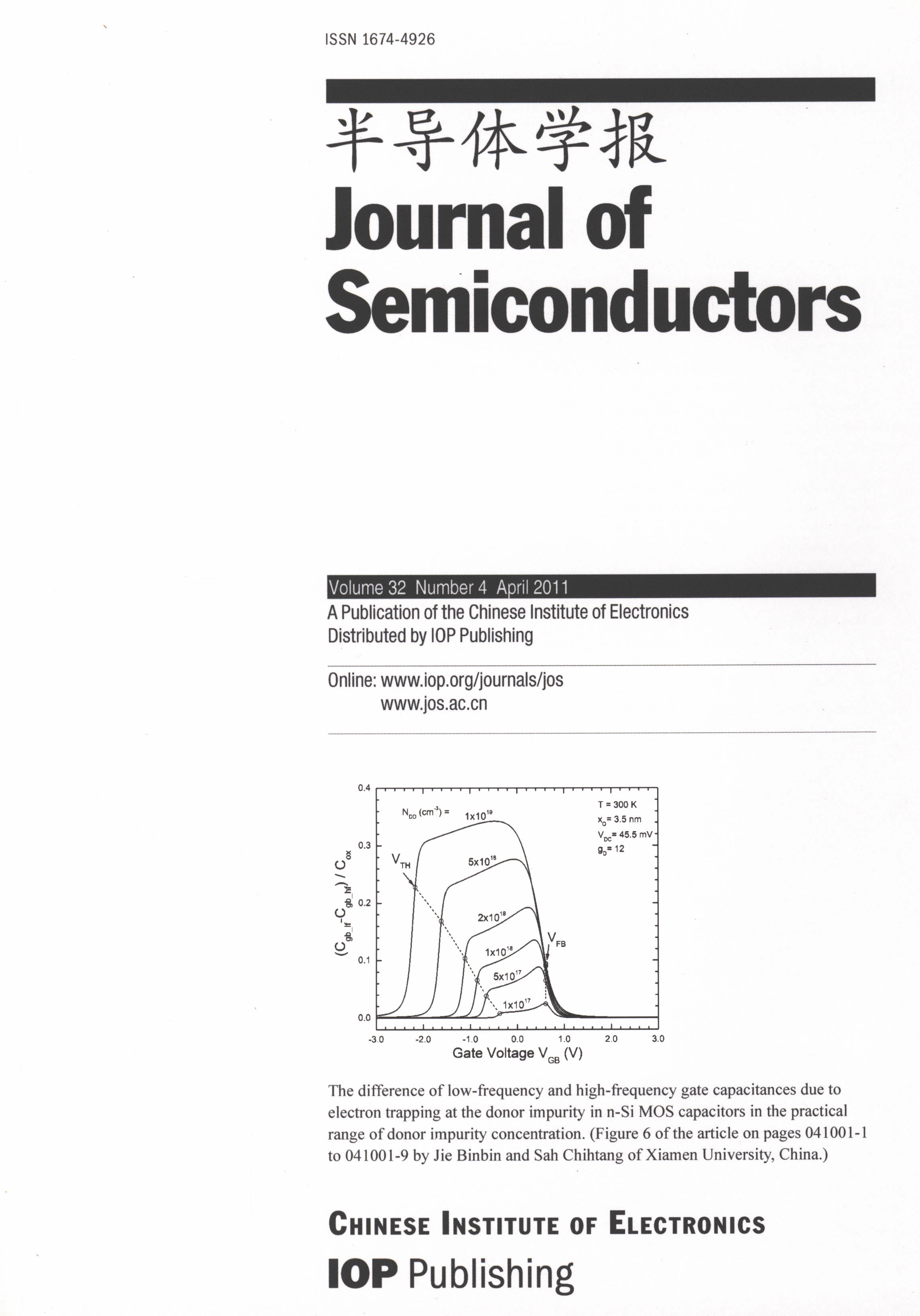
The capacitance versus DC-voltage formula from electron trapping at dopant impurity centers is derived for MOS capacitors by the charge-storage method. Fermi–Dirac distribution and impurity deionization are included in the DC-voltage scale. The low-frequency and high-frequency capacitances, and their differences and derivatives, are computed in the presence of an unlimited source of minority and majority carriers. The results show that their difference and their DC-voltage derivatives, are large and readily measurable, hence suitable as a method for characterizing the electronic trapping parameters at dopant impurity centers and for a number of lower power signal processing and device technology monitoring applications.
Issue Browser
Volume 32, Issue 4,
Apr 2011
J. Semicond.
2011, 32(4): 042001 doi: 10.1088/1674-4926/32/4/042001
The ground state binding energies of hydrogenic impurities in strained wurtzite AlxGa1-xN/GaN/AlyGa1-yN quantum wells are calculated numerically by a variational method. The dependence of the binding energy on well width, impurity location and Al concentrations of the left and right barriers is discussed, including the effect of the built-in electric field induced by spontaneous and piezoelectric polarizations. The results show that the change in binding energy with well width is more sensitive to the impurity position and barrier heights than the barrier widths, especially in asymmetric well structures where the barrier widths and/or barrier heights differ. The binding energy as a function of the impurity position in symmetric and asymmetric structures behaves like a map of the spatial distribution of the ground state wave function of the electron. It is also found that the influence on the binding energy from the Al concentration of the left barrier is more obvious than that of the right barrier.
J. Semicond.
2011, 32(4): 042002 doi: 10.1088/1674-4926/32/4/042002
A new model of a triple-terminal quantum ring with three arms is proposed. We develop an equivalent method for reducing the triple-terminal quantum ring to the double-terminal quantum ring and calculate the persistent spin currents in this model. The results indicate that the persistent spin currents show behavior of nonperiodic and unequal amplitude oscillation with increasing semiconductor ring size when the total magnetic flux is zero. However, when the total magnetic flux is non-zero, the persistent spin currents make periodic equal amplitude oscillations with increasing AB magnetic flux intensity. At the same time, the two kinds of spin state persistent spin currents have the same frequency and amplitude but the inverse phase. In addition, the Rashba spin-orbit interaction affects the phase and the phase difference of the persistent spin currents. The average persistent spin currents relate to the arm length and the terminal position as well as the distribution of the magnetic flux in each arm. Furthermore, our results indicate that the AB magnetic flux has different influences on the two kinds of spin state electrons.
J. Semicond.
2011, 32(4): 042003 doi: 10.1088/1674-4926/32/4/042003
Using the method combined non-equilibrium Green's function with density functional theory, the electronic transport properties of an (8, 0) carbon/boron nitride nanotube heterojunction coupled to Au electrodes were investigated. In the current voltage characteristic of the heterojunction, negative differential resistance was found under positive and negative bias, which is the variation of the localization for corresponding molecular orbital caused by the applied bias voltage. These results are meaningful to modeling and simulating on related electronic devices.
J. Semicond.
2011, 32(4): 043001 doi: 10.1088/1674-4926/32/4/043001
This paper reports the optical and electrical properties of electrochemically deposited polyaniline (PANI)/cerium oxide (CeO2) hybrid nano-composite film onto indium-tin-oxide (ITO) glass substrate. UV-visible spectroscopy and I–V characteristic were performed to study the optical and electrical parameters of the electrochemically deposited film. The film exhibited a strong absorption below 400 nm (3.10 eV) with a well defined absorbance peak at around 285 nm (4.35 eV). The estimated band gap of the CeO2 sample was 3.44 eV, higher than bulk CeO2 powder (Eg = 3.19 eV) due to the quantum confinement effect. Optical and electrochemical characteristics indicated that the electrical properties of PANI/CeO2 hybrid nanocomposite film are dominated by PANI doping.
J. Semicond.
2011, 32(4): 043002 doi: 10.1088/1674-4926/32/4/043002
Tungsten-doped zinc oxide (ZnO:W) films with low resistivity and high transmittance were successfully deposited on glass substrates by direct current magnetron sputtering at low temperature. The deposition pressure is varied from 12 to 21 Pa. The X-ray diffraction results show that all of the deposited films are polycrystalline and have a hexagonal structure with a preferred c-axis orientation. The crystallinity, morphologies and resistivity of ZnO:W films greatly depend on deposition pressure while the optical properties including optical transmittance, optical band gap as well as refractive index are not sensitive to deposition pressure. The deposited films with an electrical resistivity as low as 1.5 × 10⁻⁴ Ω·cm,sheet resistance of 6.8 \upOmega /口 and an average transmittance of 91.3% in the visible range were obtained at a deposition pressure of 21 Pa and sputtering power of 130 W.
J. Semicond.
2011, 32(4): 043003 doi: 10.1088/1674-4926/32/4/043003
This paper investigates the radial refractive index and optical and physical thicknesses of porous silicon (PS) layers prepared by pulse etching by means of reflectance spectroscopy, photoluminescence spectroscopy and scanning electron microscopy (SEM). The relationship between the radial refractive index and optical thickness of the PS sample and the position away from the etched centre along the radial direction has been analyzed in detail. With the position farther away from the etched centre, the SEM image shows that the physical thickness of the PS sample decreases slowly, whereas intensely decreases from 2.48 to 1.72 μm near the edge at a distance of 58 μm. Moreover, the radial refractive index increases, indicating that the porosity becomes smaller. Meanwhile, the reflectance spectra exhibit the less intense interference oscillations, which mean that the uniformity and interface smoothness of the PS layers become worse, and the envelope curves of photoluminescence spectra exhibit a trend of blue-shift, indicating a reduction in nanocrystal dimensions. The PS micro-cavity is prepared to study the radial optical properties of the PS layer, and the results verify that the uniformity and smoothness of the PS layer in the centre are better than those at the edge.
J. Semicond.
2011, 32(4): 043004 doi: 10.1088/1674-4926/32/4/043004
Molecular beam epitaxy growth of an InxGa1-xAs/GaAs quantum well (QW) structure (x equals to 0.17 or 0.3) on offcut (100) Ge substrate has been investigated. The samples were characterized by atomic force microscopy, photoluminescence (PL), and high resolution transmission electron microscopy. High temperature annealing of the Ge substrate is necessary to grow GaAs buffer layer without anti-phase domains. During the subsequent growth of the GaAs buffer layer and an InxGa1-xAs/GaAs QW structure, temperature plays a key role. The mechanism by which temperature influences the material quality is discussed. High quality InxGa1-xAs/GaAs QW structure samples on Ge substrate with high PL intensity, narrow PL linewidth and flat surface morphology have been achieved by optimizing growth temperatures. Our results show promising device applications for III–V compound semiconductor materials grown on Ge substrates.
J. Semicond.
2011, 32(4): 043005 doi: 10.1088/1674-4926/32/4/043005
High quality, homoepitaxial layers of 4H-SiC were grown on off-oriented 4H-SiC (0001) Si planes in a vertical low-pressure hot-wall CVD system (LPCVD) by using trichlorosilane (TCS) as a silicon precursor source together with ethylene (C2H4) as a carbon precursor source. The growth rate of 25–30 μm/h has been achieved at lower temperatures between 1500 and 1530 ℃. The surface roughness and crystalline quality of 50 μm thick epitaxial layers (grown for 2 h) did not deteriorate compared with the corresponding results of thinner layers (grown for 30 min). The background doping concentration was reduced to 2.13 × 1015 cm-3. The effect of the C/Si ratio in the gas phase on growth rate and quality of the epi-layers was investigated.
J. Semicond.
2011, 32(4): 043006 doi: 10.1088/1674-4926/32/4/043006
The grazing incidence X-ray reflectivity (GIXR) technique and atomic force microscopy (AFM) were exploited to obtain an accurate evaluation of the surfaces and interfaces for metalorganic chemical vapor deposition grown AlxGa1-xN/GaN superlattice structures. The X-ray diffraction results have been combined with reflectivity data to evaluate the layer thickness and Al mole fraction in the AlGaN layer. The presence of a smooth interface is responsible for the observation of intensity oscillation in GIXR, which is well correlated to step flow observation in AFM images of the surface. The structure with a low Al mole fraction (x=0.25) and thin well width has a rather smooth surface for the Rrms of AFM data value is 0.45 nm.
J. Semicond.
2011, 32(4): 044001 doi: 10.1088/1674-4926/32/4/044001
This paper reports on the fabrication and investigation of a surface-type organic semiconductor copper phthalocyanine (CuPc) based diode. A thin film of CuPc of thickness 100 nm was thermally sublimed onto a glass substrate with preliminary deposited metallic electrodes to form a surface-type Ag/CuPc/Au Schottky diode. The current–voltage characteristics were measured at room temperature under dark conditions. The barrier height was calculated as 1.05 eV. The values of mobility and conductivity was found to be 1.74 × 10⁻⁹cm2/(V.s) and 5.5 × 10⁻⁶Ω-1·cm-1, respectively. At low voltages the device showed ohmic conduction and the space charge limited current conduction mechanisms were dominated at higher voltages.
J. Semicond.
2011, 32(4): 044002 doi: 10.1088/1674-4926/32/4/044002
Top-contact thin film transistors (TFTs) using radio frequency (RF) magnetron sputtering zinc oxide (ZnO) and silicon dioxide (SiO2/ films as the active channel layer and gate insulator layer, respectively, were fabricated. The performances of ZnO TFTs with different ZnO film deposition temperatures (room temperature, 100oC and 200oC) were investigated. Compared with the transistor with room-temperature deposited ZnO films, the mobility of the device fabricated at 200oC is improved by 94% and the threshold voltage shift is reduced from 18 to 3 V (after 1 h positive gate voltage stress). Experimental results indicate that substrate temperature plays an important role in enhancing the field effect mobility, sharping the subthreshold swing and improving the bias stability of the devices. Atomic force microscopy was used to investigate the ZnO film properties. The reasons for the device performance improvement are discussed.
J. Semicond.
2011, 32(4): 044003 doi: 10.1088/1674-4926/32/4/044003
The electrical contact properties of Co/4H-SiC structures are investigated. A carbon interfacial layer between a Co film and SiC is used to improve the Ohmic contact properties significantly. The C film is deposited prior to Co film deposition on SiC using DC sputtering. The high quality Ohmic contact and specific contact resistivity of 2.30 × 10⁻⁶Ω·cm2 are obtained for Co/C/SiC structures after two-step annealing at 500 ℃ for 10 min and 1050 ℃ for 3 min. The physical properties of the contacts are examined by using XRD. The results indicate that the Co-based metal contacts have better structural stability of silicide phases formed after the high temperature annealing and carbon-enriched layer is produced below the contact, playing a key role in forming an Ohmic contact through the reduction of effective Schottky barrier height for the transport of electrons. The thermal stability of Au/Co/C/SiC Ohmic contacts is investigated. The contacts remain Ohmic on doped n-type (2.8 × 1018 cm-3) 4H-SiC after thermal aging treatment at 500 ℃ for 20 h.
J. Semicond.
2011, 32(4): 044004 doi: 10.1088/1674-4926/32/4/044004
We present a both theoretical and experimental investigation into the effect of array periodicity on the filtering characteristics of metal/dielectric photonic crystals (MDPhCs) with hexagonal arrays of subwavelength holes in gold/silicon dioxide films, varying the array periodicity from 6 to 8 μ m every 1 μm while the ratio of hole radius to array periodicity is kept constant (1/4). The results indicate that the reflectance spectrum is highly dependent on the array periodicity. When the array periodicity increases, the reflectance spectrum exhibits a large redshift regularly. The finite difference time domain (FDTD) simulations agree well with the experimental results. By analyzing the relationship between the position of the reflectance minimum and the array periodicity, we find that the filtering characteristics of MDPhCs have an almost linear relationship with the array periodicity under the conditions of keeping the same ratio of hole radius to array periodicity (1/4). This finding provides an effective way to control the filtering characteristics of MDPhCs, which have potential applications in optical filters, plasmonic thermal emitters and so on.
J. Semicond.
2011, 32(4): 044005 doi: 10.1088/1674-4926/32/4/044005
On the basis of the exact resultant solution of two dimensional Poisson's equations, a new accurate two-dimensional analytical model comprising surface channel potentials, a surface channel electric field and a threshold voltage for fully depleted asymmetrical dual material gate double-gate strained-Si MOSFETs is successfully developed. The model shows its validity by good agreement with the simulated results from a two-dimensional numerical simulator. Besides offering a physical insight into device physics, the model provides basic design guidance for fully depleted asymmetrical dual material gate double-gate strained-Si MOSFETs.
J. Semicond.
2011, 32(4): 044006 doi: 10.1088/1674-4926/32/4/044006
This paper presents the design and fabrication of a Lamb wave device based on ZnO piezoelectric film. The Lamb waves were respectively launched and received by both Al interdigital transducers. In order to reduce the stress of the thin membrane, the ZnO/Al/LTO/Si3N4/Si multilayered thin plate was designed and fabricated. A novel method to obtain the piezoelectric constant of the ZnO film was used. The experimental results for characterizing the wave propagation modes and their frequencies of the Lamb wave device indicated that the measured center frequency of antisymmetric A0 and symmetric S0 modes Lamb wave agree with the theoretical predictions. The mass sensitivity of the MEMS Lamb wave device was also characterized for gravimetric sensing application.
J. Semicond.
2011, 32(4): 044007 doi: 10.1088/1674-4926/32/4/044007
The high power light emitting diodes (LEDs) based on InGaN and AlGaInP individually are tested on line at temperatures from –30 to 100 ℃. The data are fitted to measure the relationship between temperature and the properties of forward voltage, relative light intensity, wavelength, and spectral bandwidth of two different kinds of LEDs. Why these properties changed and how these changes reflected on applications are also analyzed and compared with each other. The results show that temperature has a great influence on the performance and application of power LEDs. For applications at low temperature, the forward voltage rising and the peak wavelength blue-shifting must be considered; and at high temperature, the relative light intensity decreasing and the peak wavelength red-shifting must be considered.
J. Semicond.
2011, 32(4): 044008 doi: 10.1088/1674-4926/32/4/044008
The fabrication and characterization of distributed feedback (DFB) quantum cascade lasers emitting at λ ≈ 8.5 μm are reported. The first-order DFB grating structure was defined using the holographic lithography technique. Reliable dynamic single-mode emission with a side-mode suppression ratio of 20 dB and a tuning coefficient of –0.277 cm-1/K from 93 to 210 K is obtained in continuous wave mode by using high-reflectivity coating on the rear facet. The output power is over 100 mW at a temperature of 80 K.
J. Semicond.
2011, 32(4): 044009 doi: 10.1088/1674-4926/32/4/044009
An ultra compact triplexing filter was designed based on a silicon on insulator (SOI) nanowire arrayed waveguide grating (AWG) for fiber-to-the-home FTTH. The simulation results revealed that the design performed well in the sense of having a good triplexing function. The designed SOI nanowire AWGs were fabricated using ultraviolet lithography and induced coupler plasma etching. The experimental results showed that the crosstalk was less than –15 dB, and the 3 dB-bandwidth was 11.04 nm. The peak wavelength output from ports a, c, and b were 1455, 1510 and 1300 nm, respectively, which deviated from our original expectations. The deviation of the wavelength is mainly caused by 45 nm width deviation of the arrayed waveguides during the course of the fabrication process and partly caused by material dispersion.
J. Semicond.
2011, 32(4): 045001 doi: 10.1088/1674-4926/32/4/045001
This paper describes a multimode high-resolution digital pulse width modulator. This modulator, based on a novel hybrid structure, not only has a programmable duty cycle but also realizes phase modulation. A 576 ps pulse resolution is achieved based on a 13.56 MHz switching frequency for near field communication. Fabricated in a SMIC 0.18-μm EEPROM CMOS process, the total area of modulator is only 130 × 180 μm2. Measurement results validate the multi-mode modulation function and high pulse resolution.
J. Semicond.
2011, 32(4): 045002 doi: 10.1088/1674-4926/32/4/045002
A dual mode charge pump to produce an adaptive power supply for a class G audio power amplifier is presented. According to the amplitude of the input signals, the charge pump has two level output voltage rails available to save power. It operates both in current mode at high output load and in pulse frequency modulation (PFM) at light load to reduce the power dissipation. Also, dynamic adjustment of the power stage transistor size based on load current at the PFM mode is introduced to reduce the output voltage ripple and prevent the switching frequency from audio range. The prototype is implemented in 0.18 μm 3.3 V CMOS technology. Experimental results show that the maximum power efficiency of the charge pump is 79.5% @ 0.5x mode and 83.6% @ 1x mode. The output voltage ripple is less than 15 mV while providing 120 mA of the load current at PFM control and less than 18 mV while providing 300 mA of the load current at current mode control. An analytical model for ripple voltage and efficiency calculation of the proposed PFM control demonstrates reasonable agreement with measured results.
J. Semicond.
2011, 32(4): 045003 doi: 10.1088/1674-4926/32/4/045003
A rail-to-rail amplifier with constant transconductance, intended for audio processing, is presented. The constant transconductance is obtained by a constant current technique based on the input differential pairs operating in the weak inversion region. MOSFETs working in the weak inversion region have the advantages of low power and low distortion. The proposed rail-to-rail amplifier, fabricated in a standard 0.35 μm CMOS process, occupies a core die area of 75 × 183 μm2. Measured results show that the maximum power consumption is 85.37 μW with a supply voltage of 3.3 V and the total harmonic distortion level is 1.2% at 2 kHz.
J. Semicond.
2011, 32(4): 045004 doi: 10.1088/1674-4926/32/4/045004
A fully integrated direct-conversion digital satellite tuner for DVB-S/S2 and ABS-S applications is presented. A broadband noise-canceling Balun-LNA and passive quadrature mixers provided a high-linearity low noise RF front-end, while the synthesizer integrated the loop filter to reduce the solution cost and system debug time. Fabricated in 0.18 μm CMOS, the chip achieves a less than 7.6 dB noise figure over a 900–2150 MHz L-band, while the measured sensitivity for 4.42 MS/s QPSK-3/4 mode is –91 dBm at the PCB connector. The fully integrated integer-N synthesizer operating from 2150 to 4350 MHz achieves less than 1 ℃ integrated phase error. The chip consumes about 145 mA at a 3.3 V supply with internal integrated LDOs.
J. Semicond.
2011, 32(4): 045005 doi: 10.1088/1674-4926/32/4/045005
This paper reports a low noise switched-capacitor CMOS interface circuit for the closed-loop operation of a capacitive accelerometer. The time division multiplexing of the same electrode is adopted to avoid the strong feedthrough between capacitance sensing and electrostatic force feedback. A PID controller is designed to ensure the stability and dynamic response of a high Q closed-loop accelerometer with a vacuum package. The architecture only requires single ended operational amplifiers, transmission gates and capacitors. Test results show that a full scale acceleration of ± 3 g, non-linearity of 0.05% and signal bandwidth of 1000 Hz are achieved. The complete module operates from a ± 5 V supply and has a measured sensitivity of 1.2 V/g with a noise of floor of 0.8 μg/√Hz in closed-loop. The chip is fabricated in the 2 μm two-metal and two-poly n-well CMOS process with an area of 15.2 mm2. These results prove that this circuit is suitable for high performance micro-accelerometer applications like seismic detection and oil exploration.
J. Semicond.
2011, 32(4): 045006 doi: 10.1088/1674-4926/32/4/045006
A high-linearity PGA (programmable gain amplifier) with a DC offset calibration loop is proposed. The PGA adopts a differential degeneration structure to vary voltage gain and uses the closed-loop structure including the input op-amps to enhance the linearity. A continuous time feedback based DC offset calibration loop is also designed to solve the DC offset problem. This PGA is fabricated by TSMC 0.13 μm CMOS technology. The measurements show that the receiver PGA (RXPGA) provides a 64 dB gain range with a step of 1 dB, and the transmitter PGA (TXPGA) covers a 16 dB gain. The RXPGA consumes 18 mA and the TXPGA consumes 7 mA (I and Q path) under a 3.3 V supply. The bandwidth of the multi-stage PGA is higher than 20 MHz. In addition, the DCOC (DC offset cancellation) circuit shows 10 kHz of HPCF (high pass cutoff frequency) and the DCOC settling time is less than 0.45 μs.
J. Semicond.
2011, 32(4): 045007 doi: 10.1088/1674-4926/32/4/045007
This paper covers a micro sensor analog signal processing circuit system (MASPS) chip with low power and a digital signal processing circuit board implementation including hardware connection and software design. Attention has been paid to incorporate the MASPS chip into the digital circuit board. The ultimate aim is to form a hybrid circuit used for mixed-signal processing, which can be applied to a micro sensor flow monitoring system.
J. Semicond.
2011, 32(4): 045008 doi: 10.1088/1674-4926/32/4/045008
This paper presents a 4th-order reconfigurable analog baseband filter for software-defined radios. The design exploits an active-RC low pass filter (LPF) structure with digital assistant, which is flexible for tunability of filter characteristics, such as cut-off frequency, selectivity, type, noise, gain and power. A novel reconfigurable operational amplifier is proposed to realize the optimization of noise and scalability of power dissipation. The chip was fabricated in an SMIC 0.13 μm CMOS process. The main filter and frequency calibration circuit occupy 1.8 × 0.8 mm2 and 0.48 × 0.25 mm2 areas, respectively. The measurement results indicate that the filter provides Butterworth and Chebyshev responses with a wide frequency tuning range from 280 kHz to 15 MHz and a gain range from 0 to 18 dB. An IIP3 of 29 dBm is achieved under a 1.2 V power supply. The input inferred noise density varies from 41 to 133 nV/√Hz according to a given standard, and the power consumptions are 5.46 mW for low band (from 280 kHz to 3 MHz) and 8.74 mW for high band (from 3 to 15 MHz) mode.
J. Semicond.
2011, 32(4): 045009 doi: 10.1088/1674-4926/32/4/045009
A fully pipelined 10 B/8 B decoder is presented with shorter critical path than before, and so its speed is improved greatly. Based on the proposed architecture, a 10 B/8 B decoder is implemented based on standard cells in 0.18 μm CMOS technology with a core area of 375 × 375 μ m2. Measurement results show that the decoder works well and its speed can be up to 6.25 Gbps. At a 1.8 V power supply, the total power consumption is 21.6 mW during 6.25 Gbps operation and the peak-to-peak jitter in the eye diagram is 177.8 ps.
J. Semicond.
2011, 32(4): 045010 doi: 10.1088/1674-4926/32/4/045010
A PLL clock generator with reconfigurable multi-functions for FPGA design applications is presented. This clock generator has two configurable operation modes to achieve clock multiplication and phase alignment functions, respectively. The output clock signal has advanced clock shift ability such that the phase shift and duty cycle are programmable. In order to further improve the accuracy of phase alignment and phase shift, a VCO design based on a novel quick start-up technique is proposed. A new delay partition method is also adopted to improve the speed of the post-scale counter, which is used to realize the programmable phase shift and duty cycle. A prototype chip implemented in a 0.13-μm CMOS process achieves a wide tuning range from 270 MHz to 1.5 GHz. The power consumption and the measured RMS jitter at 1 GHz are less than 18 mW and 9 ps, respectively. The settling time is approximately 2 μs.
J. Semicond.
2011, 32(4): 045011 doi: 10.1088/1674-4926/32/4/045011
A nanopower switched-capacitor CMOS sub-bandgap voltage reference has been implemented using a Chartered 0.35-μm 3.3-V/5-V dual gate mixed-signal CMOS process. The proposed circuit generates a precise sub-bandgap voltage of 1 V. The temperature coefficient of the output voltage is 13.4 ppm/℃ with the temperature varying from –20 to 80 ℃. The proposed circuit operates properly with the supply voltage down to 1.3 V, and consumes 150 nA at room temperature. The line regulation is 0.27%/V. The power supply rejection ratio at 100 Hz and 1 MHz is –39 dB and –51 dB, respectively. The chip area is 0.2 mm2.
J. Semicond.
2011, 32(4): 045012 doi: 10.1088/1674-4926/32/4/045012
A novel integration-based yield estimation method is developed for yield optimization of integrated circuits. This method tries to integrate the joint probability density function on the acceptability region directly. To achieve this goal, the simulated performance data of unknown distribution should be converted to follow a multivariate normal distribution by using Box-Cox transformation (BCT). In order to reduce the estimation variances of the model parameters of the density function, Orthogonal Array-based Modified Latin Hypercube Sampling (OA-MLHS) is presented to generate samples in the disturbance space during simulations. The principle of variance reduction of model parameters estimation through OA-MLHS together with BCT is also discussed. Two yield estimation examples, a fourth-order OTA-C filter and a 3-dimensional quadratic function, are used for comparison of our method with Monte Carlo based methods including Latin Hypercube Sampling and Importance Sampling under several combinations of sample sizes and yield values. Extensive simulations show that our method is superior to other methods with respect to accuracy and efficiency under all the given cases. Therefore, our method is more suitable for parametric yield optimization.
J. Semicond.
2011, 32(4): 046001 doi: 10.1088/1674-4926/32/4/046001
An electroless deposition (ELD) method is introduced to fabricate a metal nanoplug for its advantages of simplicity, low cost and auto-selectivity. It was demonstrated that nanoplugs of less than 50 nm in diameter can be fabricated by ELD nickel on various substrates, such as silicon, tungsten and titanium nitride. The main composition of the ELD nanoplug was characterized as nickel by an energy dispersive X-ray microanalyzer. A functional vertical phase-change random access memory (PCRAM) device with a heater diameter of around 9 μm was fabricated by using the ELD method. The I–V characteristics demonstrated that the threshold current is only 90.8 μA. This showed that the ELD process can satisfy the demands of PCRAM device application, as well as device performance improvement. The ELD process provides a promising method for the simple and low-cost fabrication of metal nanoplugs.